In this video I identify the root cause of the IGBT failures, to a wrong gate driver IC. With the correct gate driver IC, full-bridges repaired with tested IGBTs, we can finally finish the static load test and adjust phase lead compensation on the Tesla coil.
This is the 5th article / video in the series of designing and building a DRSSTC Tesla coil from scratch, with focus on being easy and cheap, for you to replicate. You can find the previous information in these articles:
- Designing A Complete DRSSTC Tesla Coil In 10 Minutes
- Building the 10 Minute DRSSTC Part 1: Finding the Components
- Building the 10 Minute DRSSTC Part 2: Construction and Assembly
- Testing the 10 Minute DRSSTC Part 1: UD2.9 Driver and DC Bus Capacitors
- Exploding the 10m Design DRSSTC: Softstart, Secondary Coil Terminations and Total Annihilation
Problems with the UD2.9 Driver
I had accidently ordered UCC27524P gate driver ICs, which is the wrong non-inverting input type of that gate driver series. It needed to be the UCC27423 or UCC27523 with inverting input logic. This mistake is not obvious when bench testing, as we force a feedback signal to the driver, but it will keep it for starting up on its own from feedback CT on the primary circuit. I had some old 27423 drivers ICs in a box, marked with a U, no TI logo. To my surprise these are maybe over 25 years old, as Unitrode was bought up by Texas Instruments, back in the 1990s.
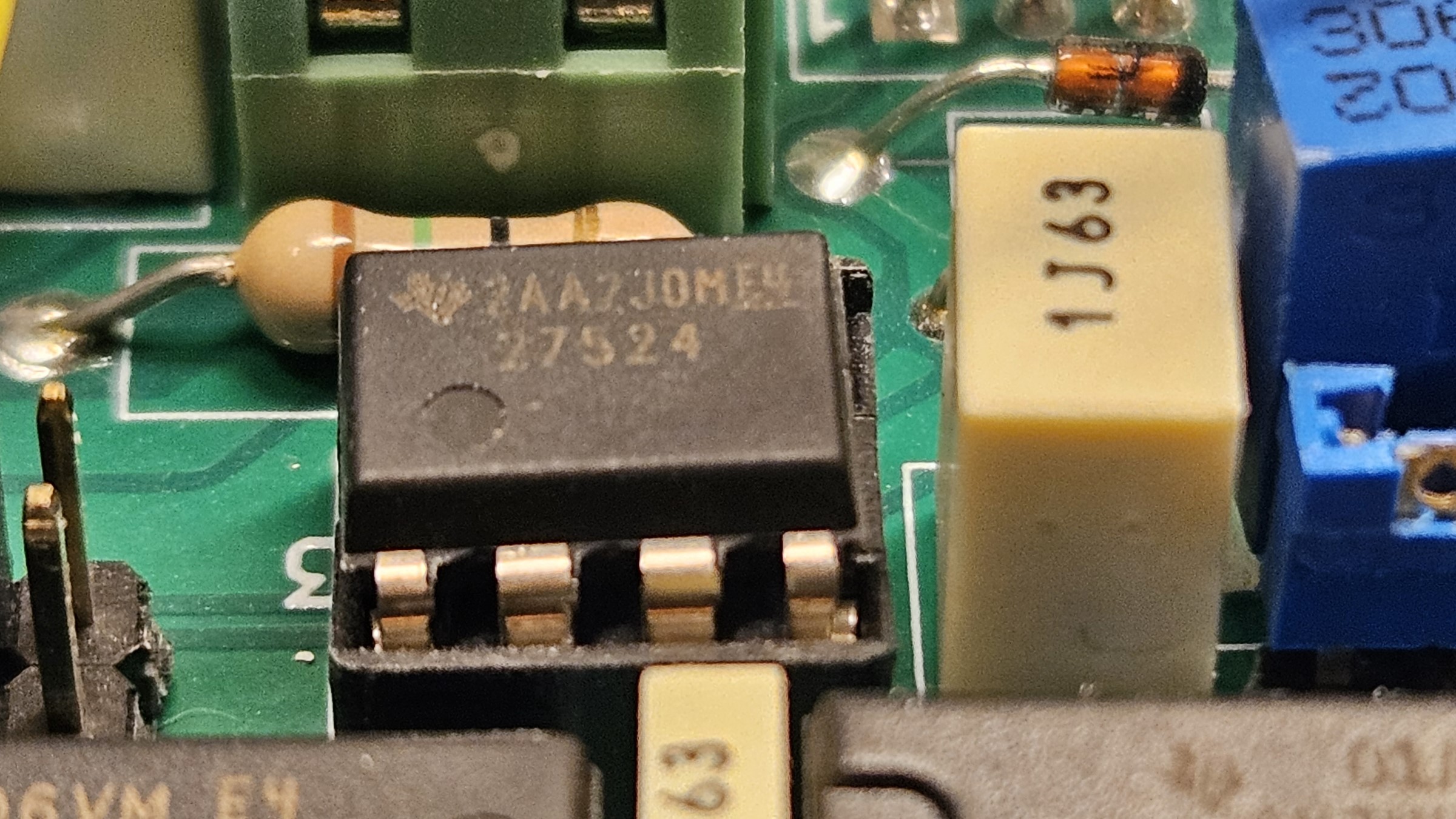
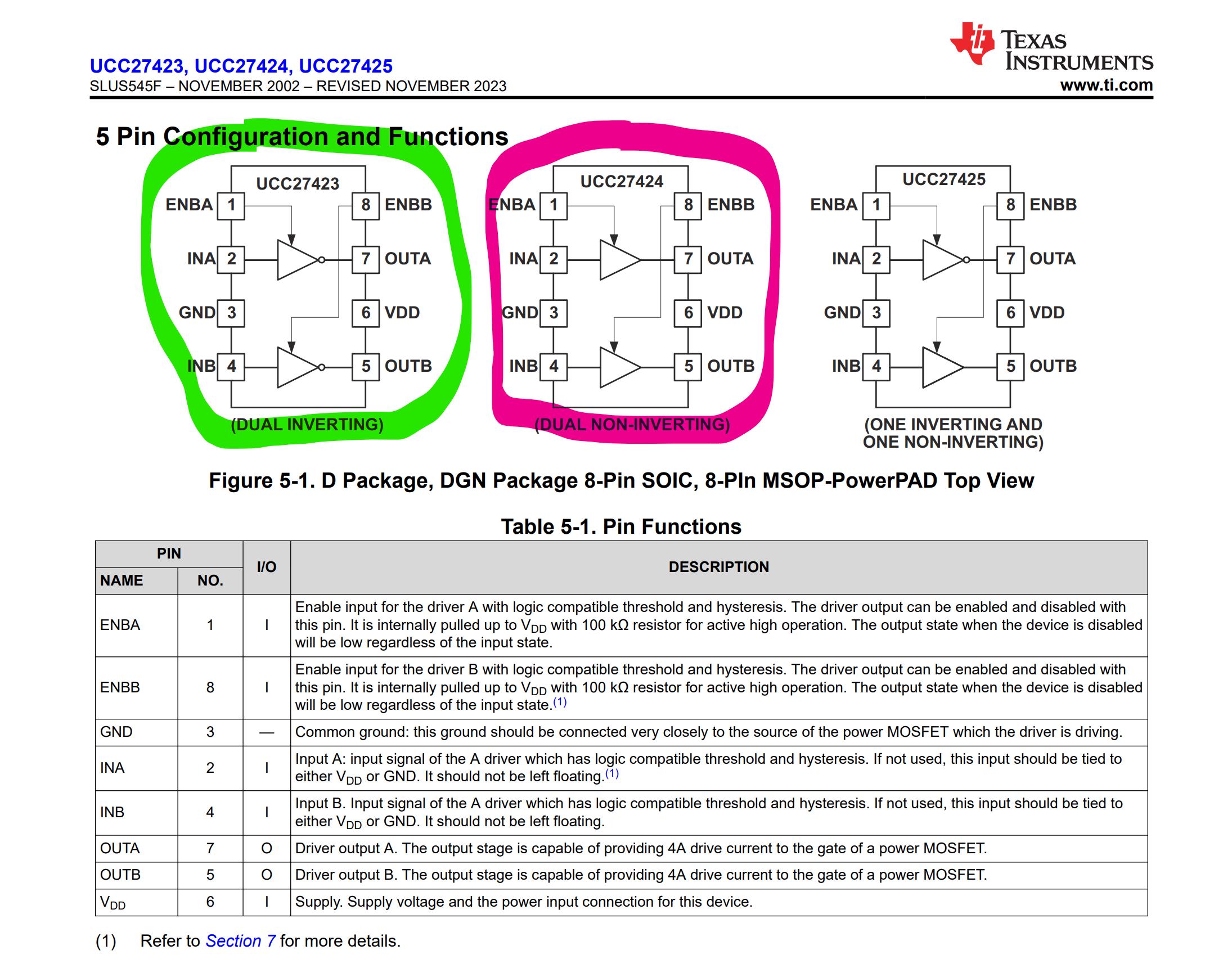

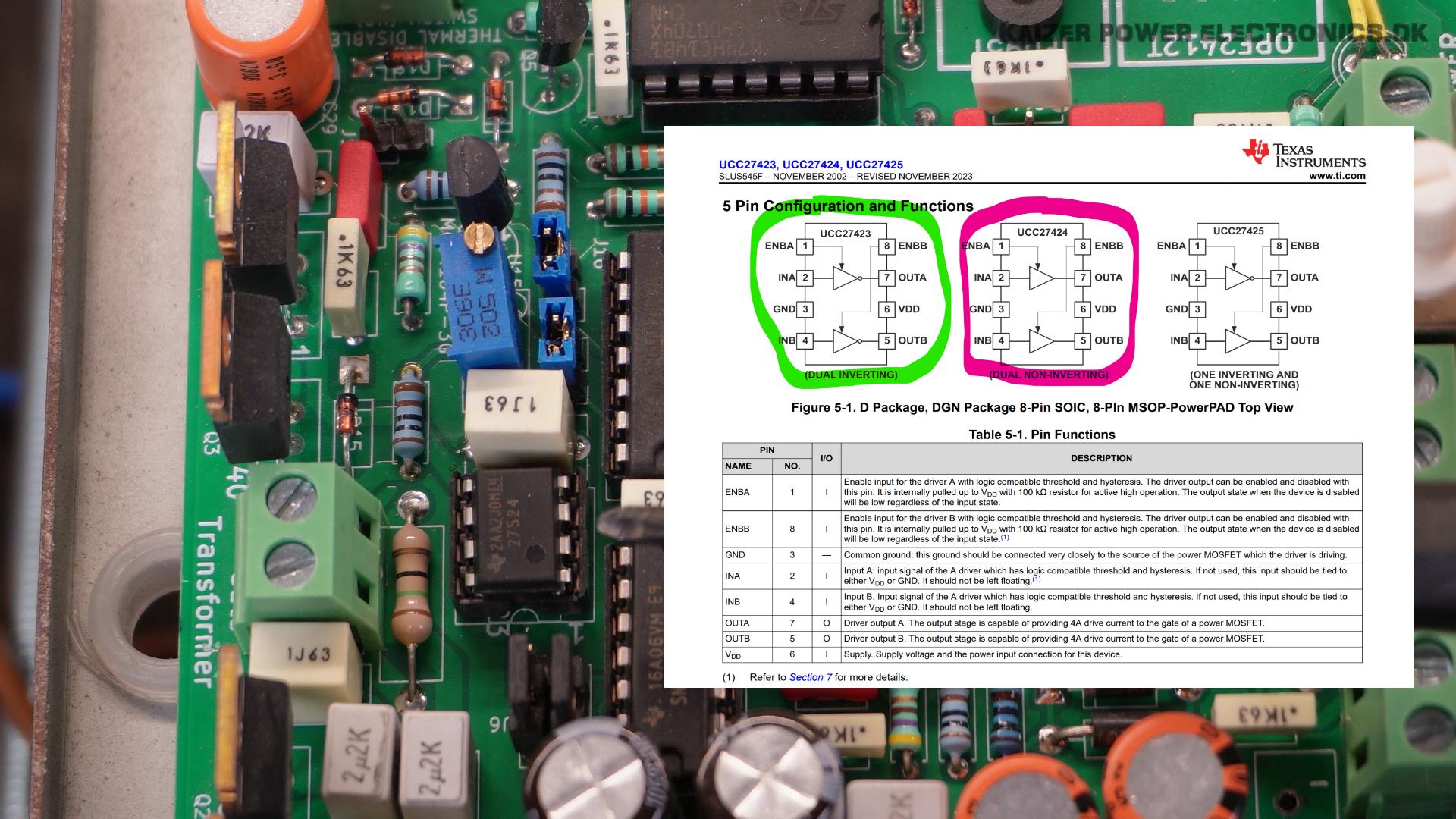
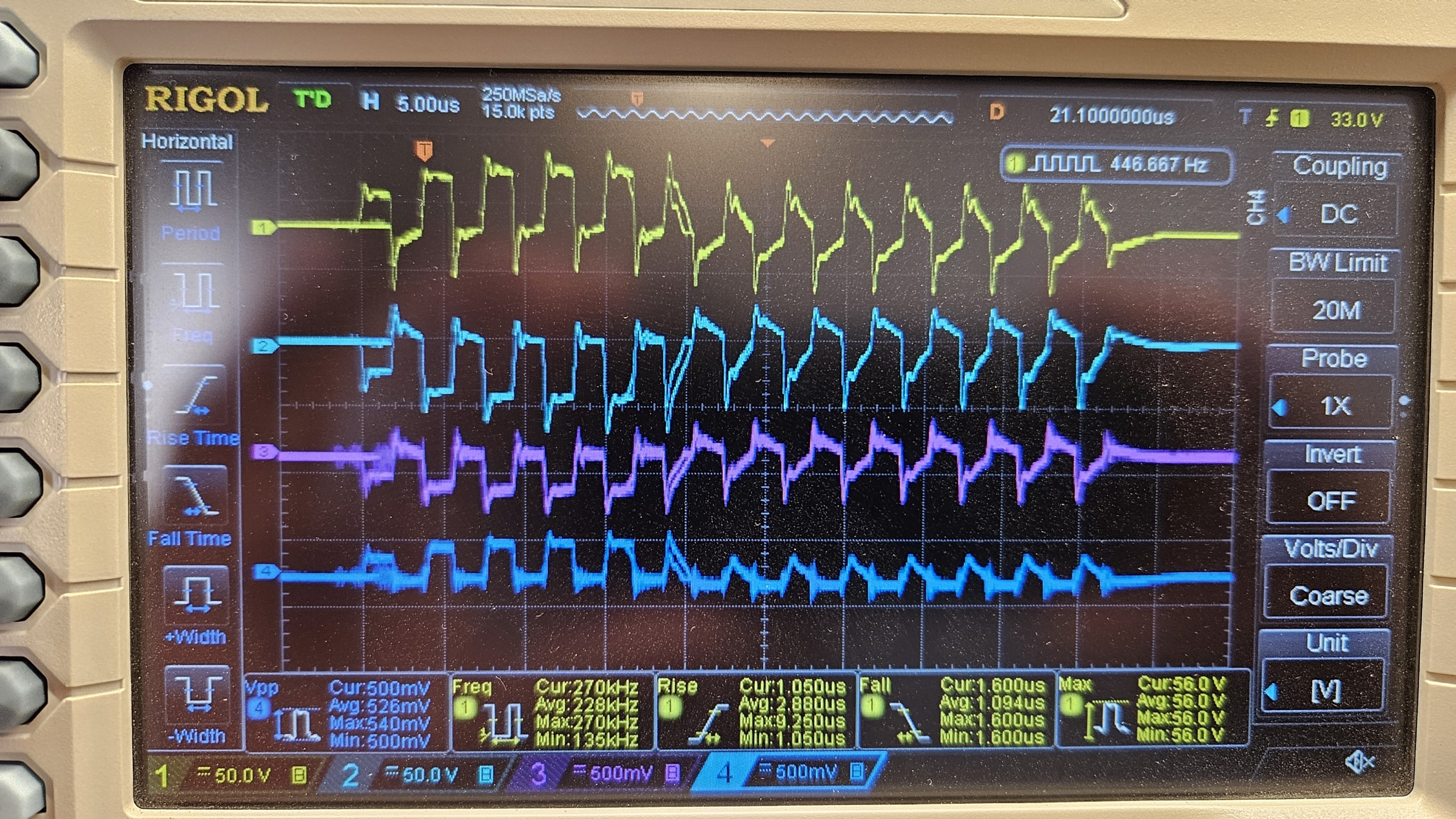
I also learned that this wrong gate driver IC could actually destroy the IGBTs, even without any supply on the DC bus. When bench testing the new full-bridges, gate drive waveform suddenly started acting weird and then flatlined. Short-circuit testing the full-bridge showed that it was damaged again. This damage was therefore already present in the previous episode, where I force the coil to run with a signal generator and the explosion is no longer a mystery 🙂
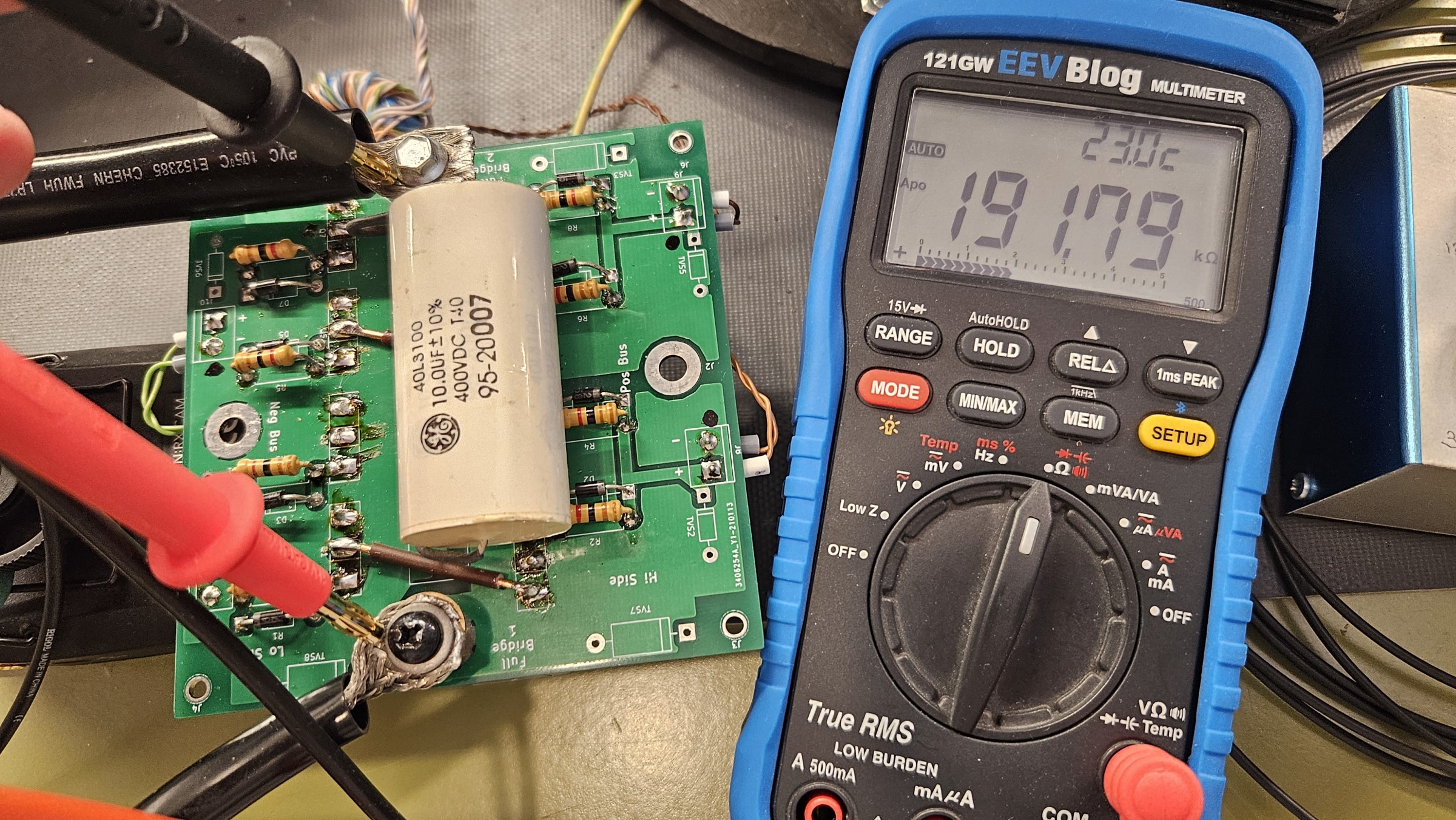
Destroyed Full-bridges, IGBT Test and New Bridges
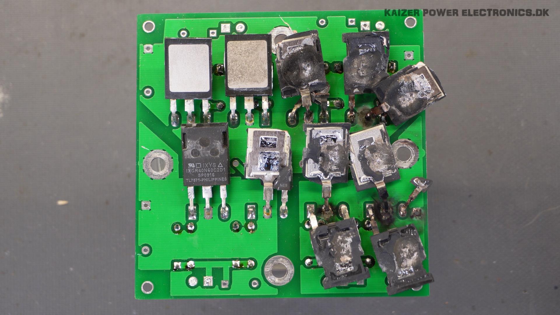
The full-bridge that exploded in the previous episode, shows clearly that dies are completely melted on two IGBTs from lower and high side of the bridge. It is quite surprising that the packages did not even crack, yet are so melted into large blobs on the inside.
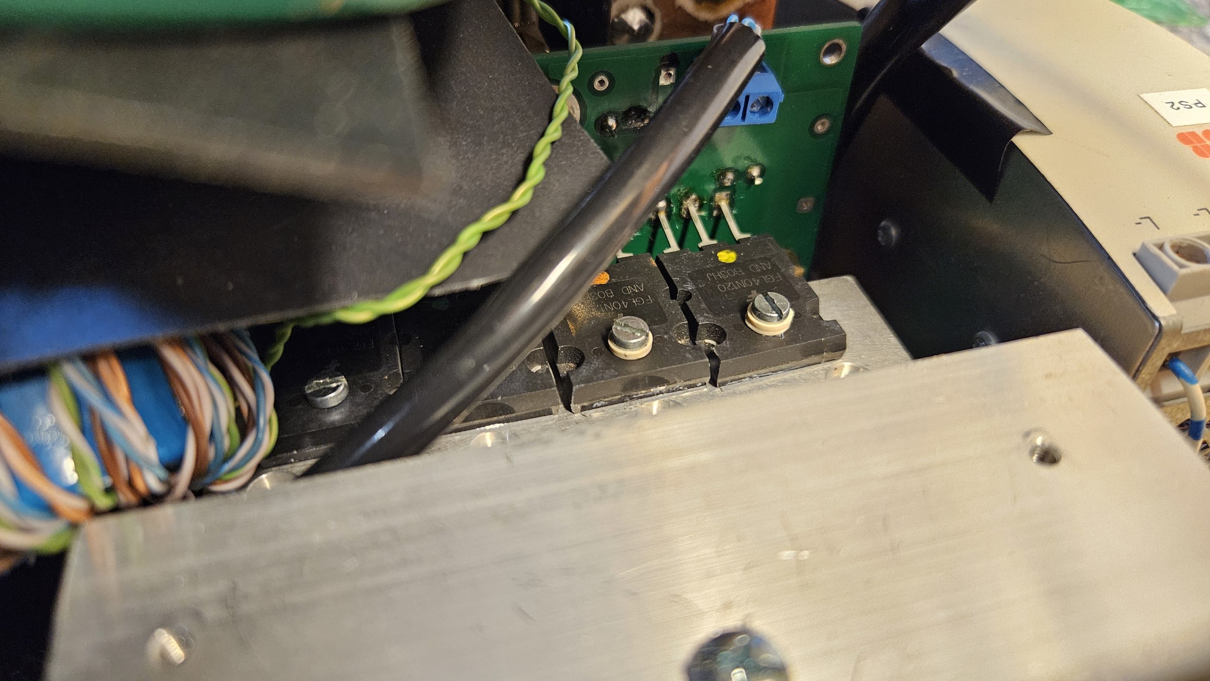
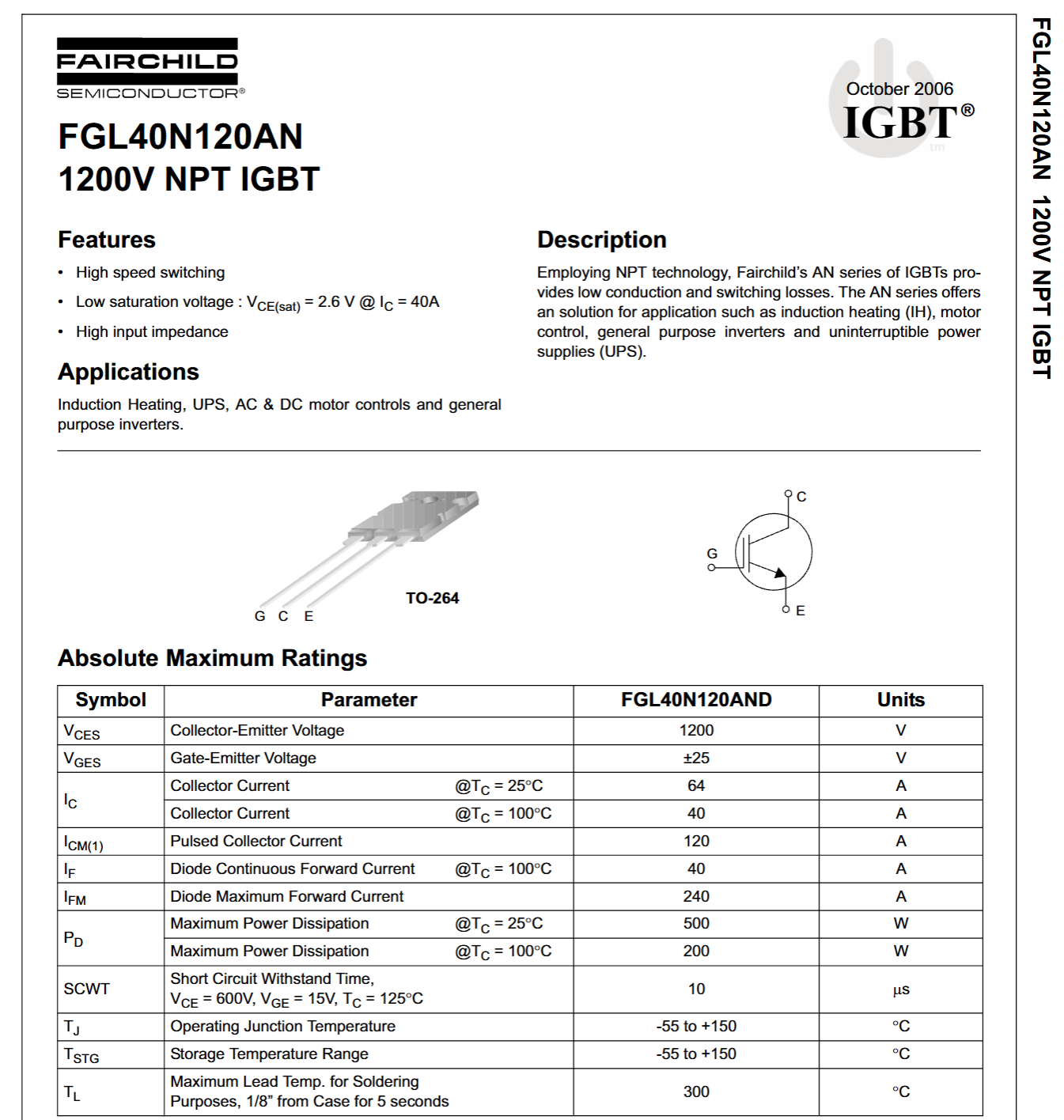
I only had enough 40N60 IGBTs to exchange both full-brigdes once. I wanted to compare the wrong IC vs. correct IC, but that actually destroyed the IGBTs in one of the bridges again. Having run out of 40N60, I had to substitute with some FGL40N120AN IGBTs, but these have lower current handling capability and higher gate capacitances, from the double voltage rating.
| Name | Voltage | Current (25C) | Peak Current | Vce(sat) | Switch losses Etotal (mJ) |
| 40N60 | 600 V | 80 A | 120 A | 2.5 V | 1.61 |
| FGL40N120AN | 1200 V | 40 A | 160 A | 2.6 V | 4.3 |
I changed the two small capacitors 0.1 uF and 0.47 uF, to a single large 10 uF snubber capacitor, to counter for the relatively high stray inductances in the full-bridges layout.
I added two pieces of copper wire, to bridge through the vias between the IGBTs, to get a better suited high current path for the resonant primary circuit.
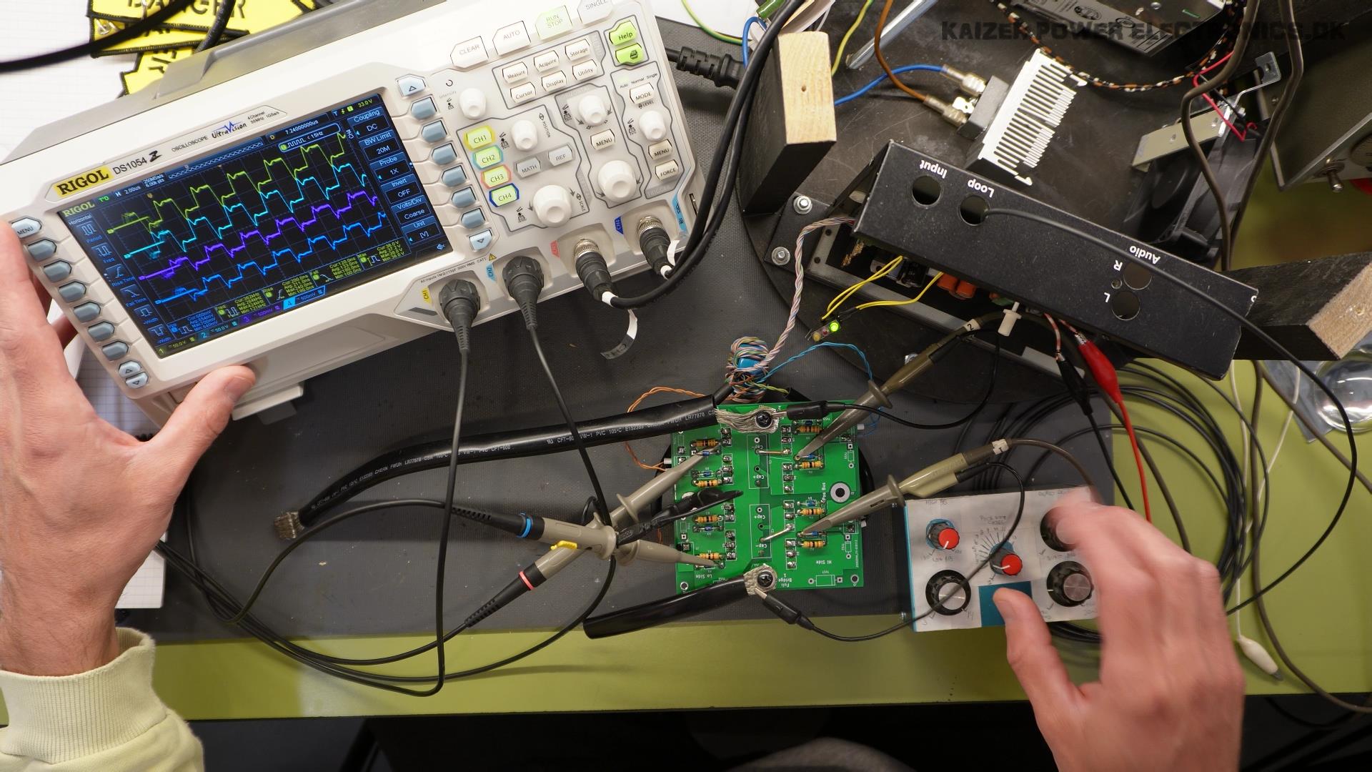
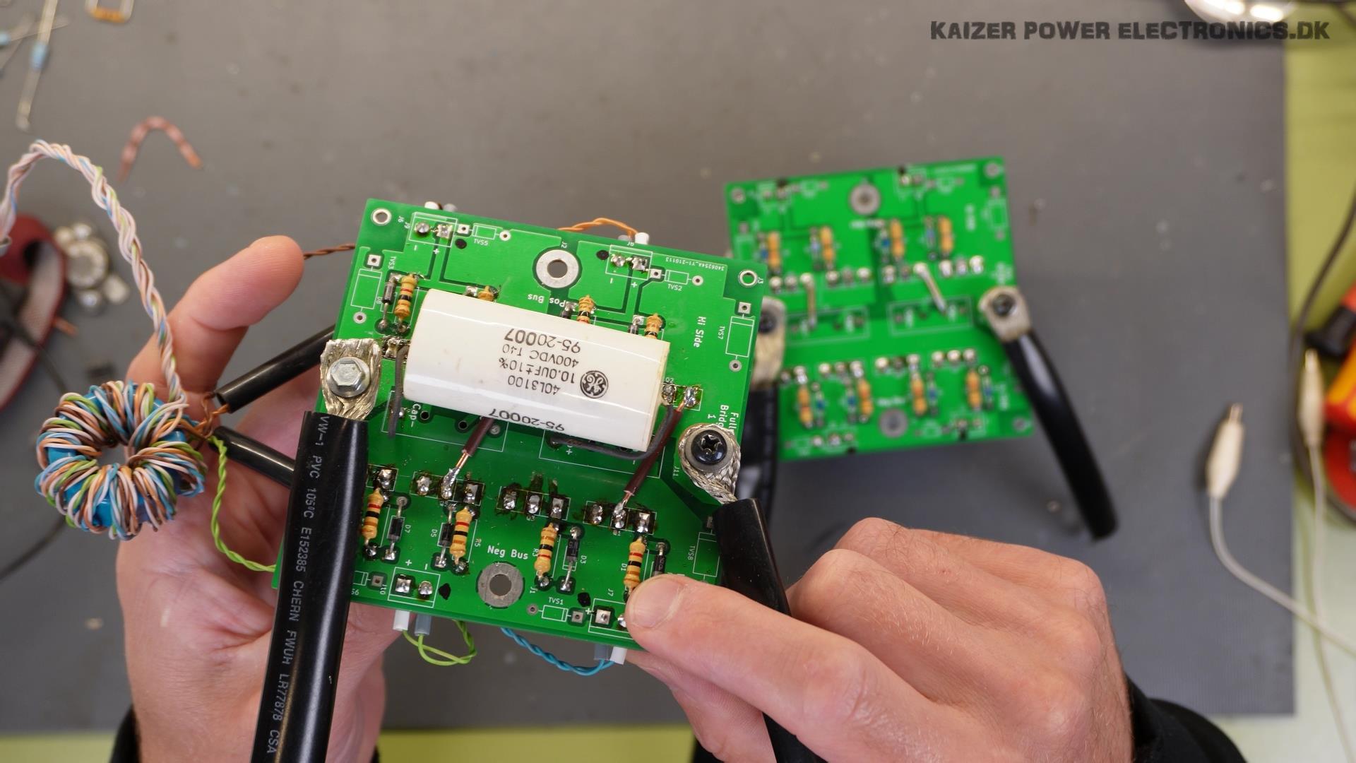
DRSSTC Primary Waveforms and Phase Lead Adjustment
Measurements with current monitors and differential probes is pretty straight forward. Place your current transformer on the lead from inverter output to primary circuit and place the differential probe for voltage measurement on the two inverter outputs.
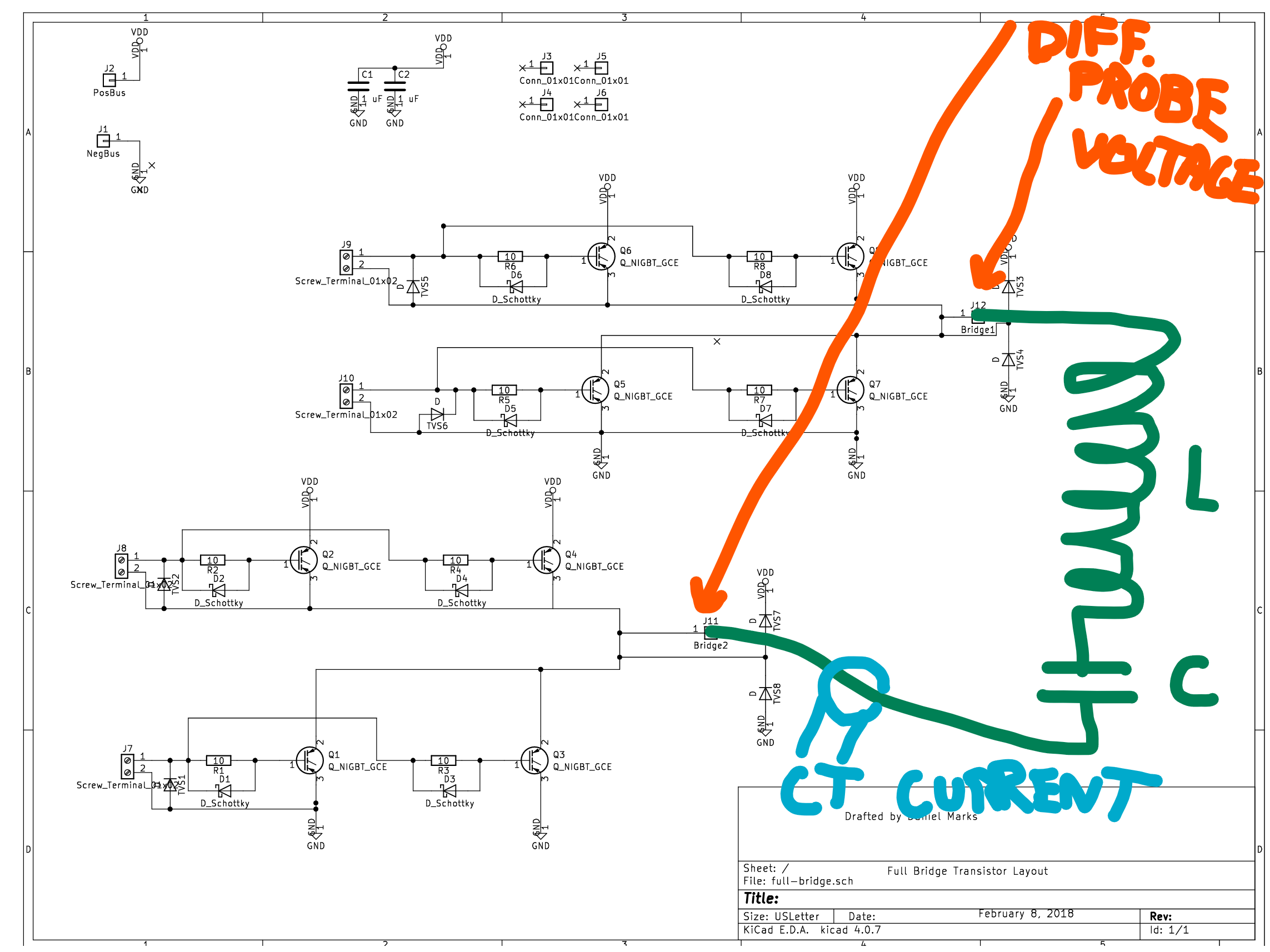
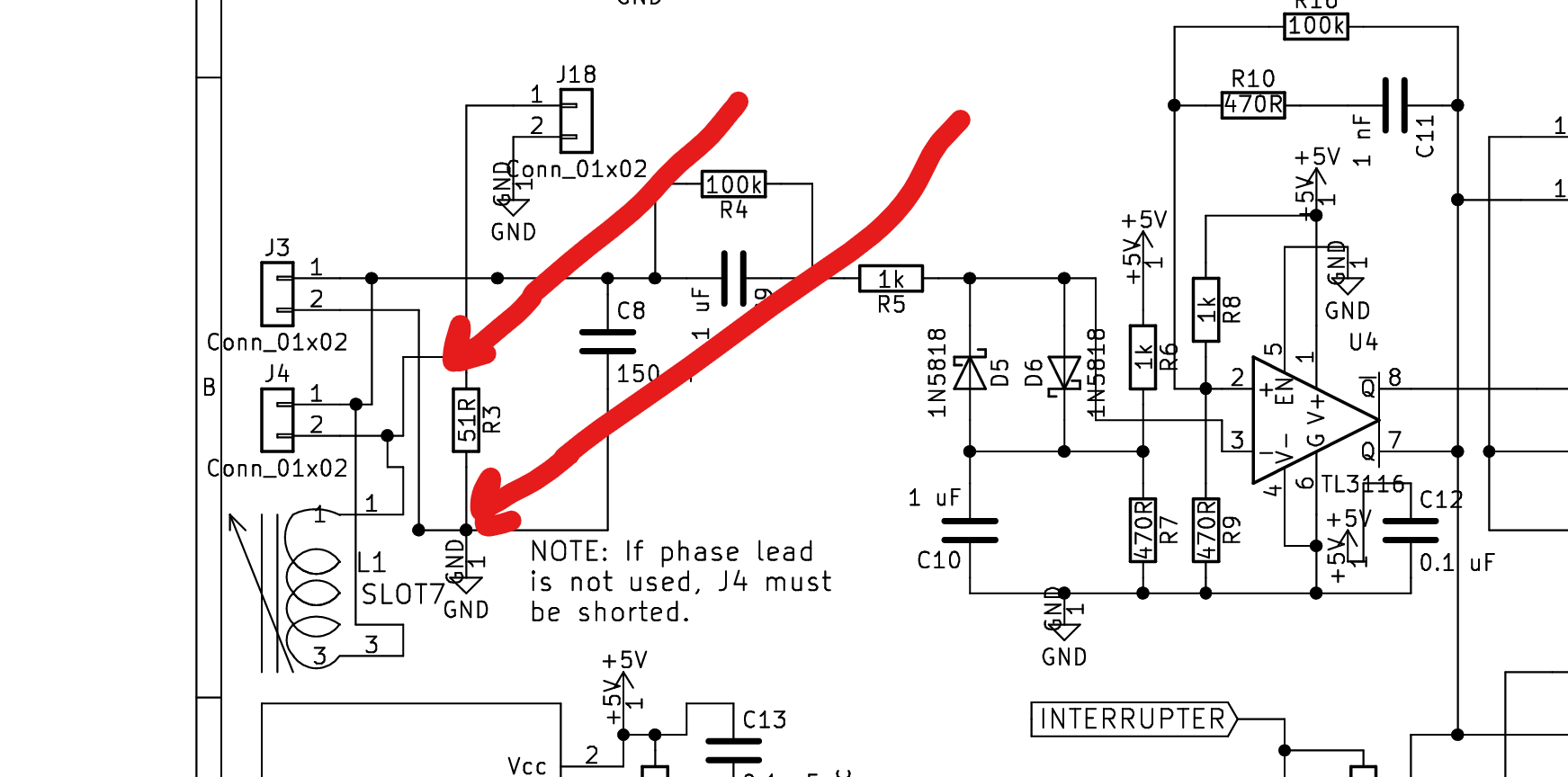
Alternative measurements, if you do not own expensive tools like current monitors and differential probes, is to use a normal 2-channel oscilloscope with 10x probes. You have to be very careful with placing the grounding clips correctly according to the schematics, else you short out your full-bridge lower leg.
For current measurement, place a probe across the shunt resistor R3 on the driver, excluding the inductor! This is important to not get phase
lead into your current signal that you are trying to “move” the voltage in regard to.
For the voltage measurement, place a probe across one of the lower leg IGBTs collector and emitter legs, the voltage here is only half of your DC bus. This does not represent voltage spikes on the high side of the full-bridge, but it should be sufficient to get a fair phase lead adjustment.

Blue trace is primary current with a scale of 100A/div and yellow trace is inverter output voltage with a scale of 250V/div. The primary current is in some screenshots set to 200A/div, in the screenshots where it is on level with the yellow trace.
The blue waveform shows the primary current ringing up and down. The yellow traces shows where the interrupter goes off again, the reverse voltage action is seen and the current is ringing down again from this point.
The sloped inverter output voltage waveform, is an indication of high stray inductances in the primary circuit layouts. The tracks or connections from DC bus capacitors to the primary coil connections, have to be as low inductance as possible. This PCB layout could use improvements in the track width and getting DC bus positive and negative tracks opposing each other, to cancel out the inductance.
The pulse skipping feature of the driver results in the OCD never really kicking in. The screenshot shows two pulse skipping events, the ringing current is halted by stopping the driver for one cycle, restarting from scratch and that results in what looks like 3 separate low duty-cycle pulses.
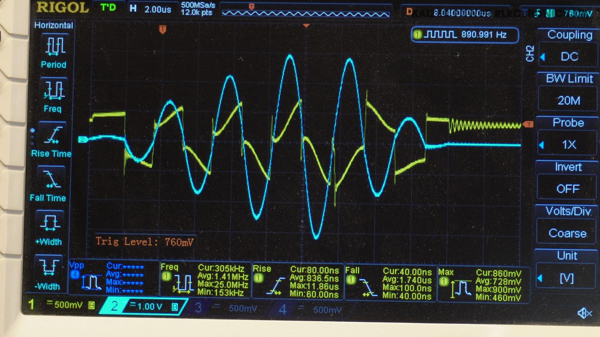
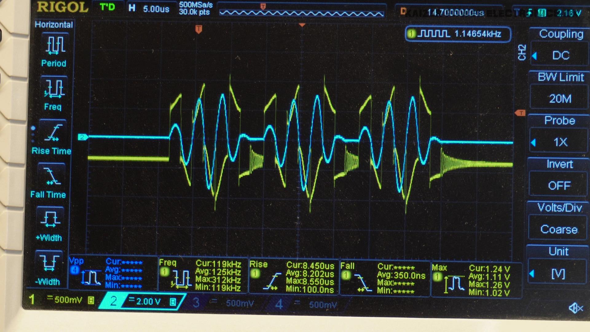
Phase lead adjustment is quite simple, you turn the adjustable inductor either left or right and watch the waveforms for a change. You want to find the spot where the spikes at the start of the voltage waveform is as low as possible.
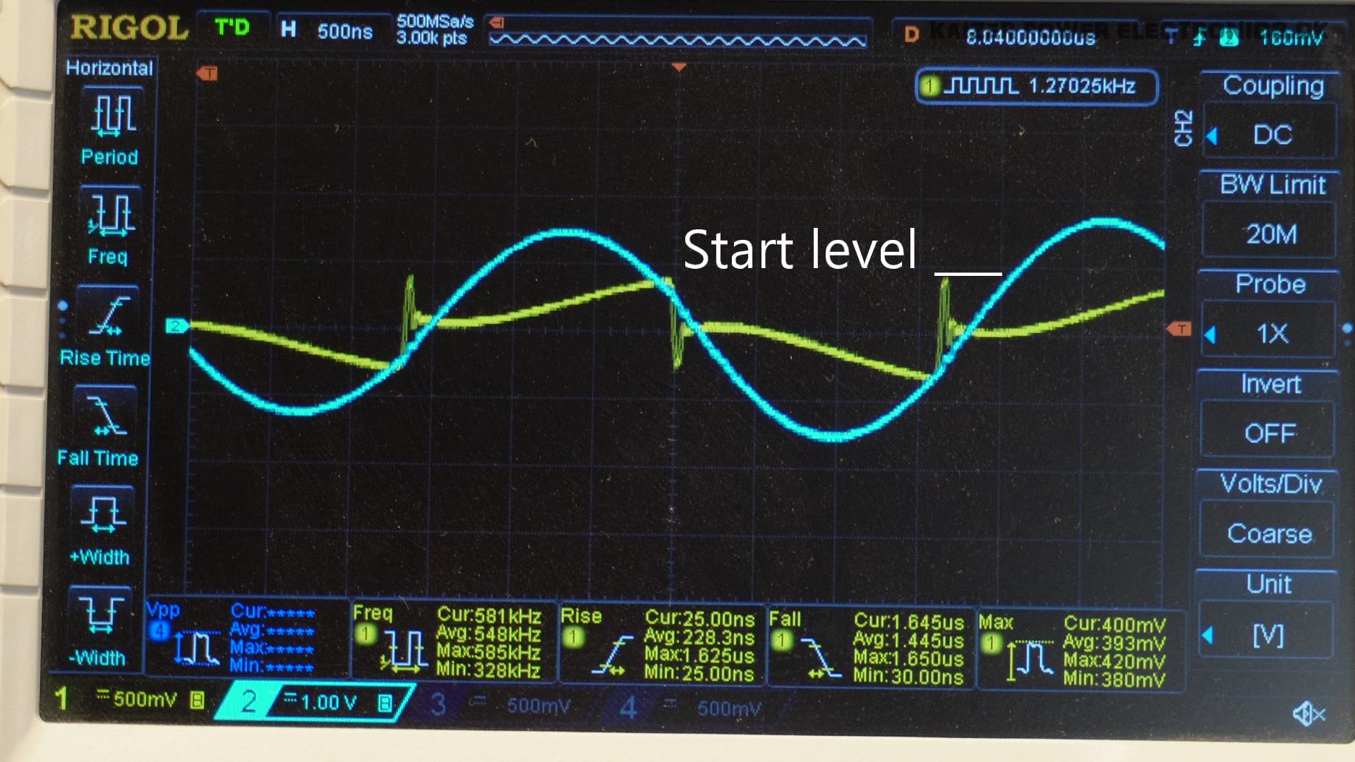
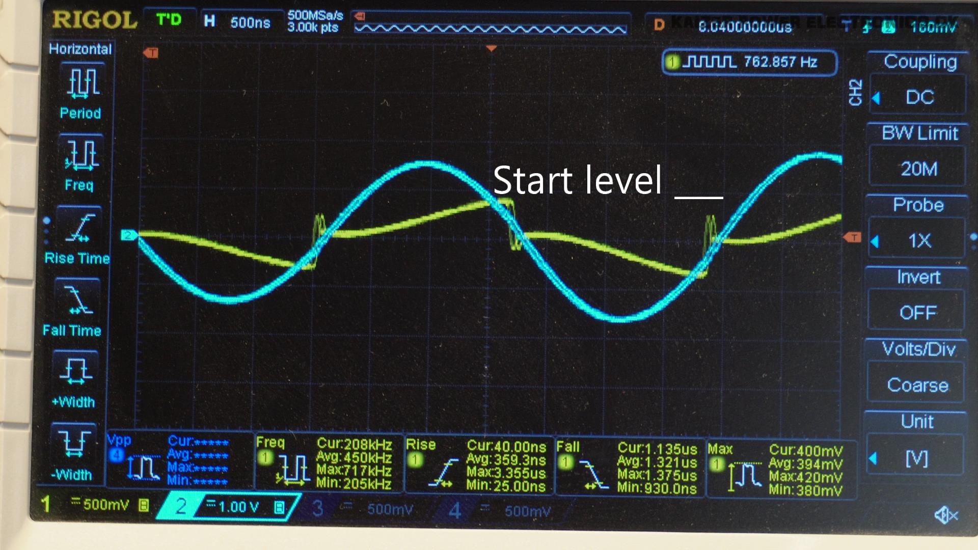
If adjusting the inductance is not making any change to the waveform, maybe the inductor size or type is not suitable. To check your variable inductor, you can use this calculator I made for this purpose: https://kaizerpowerelectronics.dk/calculators/ud2-x-phase-lead-calculator/