This is a summary of the whole project from design, to building and to test the “10 minute design DRSSTC Tesla Coil”. This article will eventually be populated with the information, from the underlying posts of design and building progress.
- Designing: Designing A Complete DRSSTC Tesla Coil In 10 Minutes
- Building part 1: Building the 10 Minute DRSSTC Part 1: Finding the Components
- Building part 2: Building the 10 Minute DRSSTC Part 2: Construction and Assembly
- Testing: Testing the 10 Minute DRSSTC Part 1: UD2.9 Driver and DC Bus Capacitors
- Running: Exploding the 10m Design DRSSTC: Softstart, Secondary Coil Terminations and Total Annihilation
- Rebuilding part 1: Rebuilding the 10 Minute Design DRSSTC, Static Test and Phase Lead Adjustment
- Rebuilding part 2: Rebuilding the 10 Minute Design DRSSTC: No More TO-247 IGBTs
Introduction
The idea to design a DRSSTC dates back to 14th February 2021, following a brainstorm session on what projects/videos to make, it did however strand on my TODO list for quite some years. The design video was recorded on the 8th February 2026, almost 5 years after the idea was scribbled down!
Safety
WARNING!: Working with electricity is dangerous, all information found on my site is for educational purpose and I accept no responsibility for others actions using the information found on this site.
Read this document about safety! http://www.pupman.com/safety.htm
Specifications
This is a list of the most important and major parts of a DRSSTC. It is not a complete list of every part needed and some parts have changed from design to end product.
| Description | Amount | |
| Supply voltage | 230 VAC ~ 320 VDC | |
| Bridge topology | Full-bridge 2x parallel PCB | 1 |
| IGBTs | TO-247, 40N60, 600 V, 80/120 A | 8 |
| Rectifier | 25 A full-bridge | 1 |
| Driver | UD2.9 pulse skip PCB | 1 |
| Interrupter | 555 timer based PCB | 1 |
| Secondary coil | 230 x 75 mm, 1000 windings, 0.2 mm | 1 |
| Topload | 300 mm major, 75 mm minor diameter | 1 |
| Resonant frequency | Around 300 kHz | |
| Primary coil | 4-5 turns of 5 mm copper brake line | 1 |
| MMC | CJE 0.1 uF, 3000 VAC, 80 A MKP capacitor | 1 |
| DC bus capacitors | 1500 uF, 450 VDC, electrolytic capacitor | 6 |
| Snubber capacitor | 2.2 uF, 275 VAC / 450 VDC, MKP capacitor | 1 |
For indepth knowledge on Tesla coils and DRSSTC in particular, I recommend reading the entire guide: https://kaizerpowerelectronics.dk/tesla-coils/drsstc-design-guide/ For the purpose of this video / project, to design something really fast, I will skip to selected parts of the guide.
A Tesla Coil is primarily defined by its secondary coils characteristics. So the first goto is the DRSSTC Design Guide part on secondary coils: http://kaizerpowerelectronics.dk/tesla-coils/drsstc-design-guide/secondary-coil/ and scroll to the header “How to find the right secondary coil size and ratio”, select a size suitable to your needs and available components. Scroll further down to “How to find the right secondary coil wire size and number of turns” for selection of impedance, according to chosen wire size and number of windings. I chose a secondary coil with diameter of 75 mm, 1000 turns of 0.2 mm diameter copper wire, resulting in a winding that is 220-230 mm long.
The easy way to choose a toroid topload, that I find to have the “right” proportions”, is to use the secondary coil dimensions for the topload as well. Secondary coil diameter = topload minor diameter and secondary winding length = topload major diameter. I chose a toroid topload with minor diameter 75 mm and major diameter 300 mm.
Calculate the toroid topload capacitance: https://deepfriedneon.com/tesla_f_calctoroid.html which comes out to 13 pF.
Verify your secondary coil numbers in the helical coil calculator and use the topload capacitance to get the resonant frequency of the secondary system: https://kaizerpowerelectronics.dk/calculators/helical-coil-calculator/ . Resonant frequency comes out very close to 300 kHz.
I wanted to use the DRSSTC PCB pack from profdc9 ( https://highvoltageforum.net/index.php?topic=353.0 ), as it contains interrupter, UD2.7c and UD2.9 drivers and 4 different bridge layouts. I went with the largest, full-bridge of parallel TO-257 IGBTs.
Choose an IGBT. Follow the guide for the complex calculations or rip it with finding a IGBT with similar ratings to 40N60 for TO-247 devices (400 A) or if choosing bricks, you can go with 2-3 times its pulsed current rating as your maximum design goal. I want to use a full-bridge of parallel IGBTs, so I bump my peak rating up to 600 A. With parallel devices, you can never assume do double the current handling, due to possible uneven current sharing.
Select a resonant capacitor size, also called a MMC, if its constructed from multi mini capacitors. https://kaizerpowerelectronics.dk/tesla-coils/drsstc-design-guide/mmc-tank-capacitor/ scroll down to “How to choose the value of the MMC capacitance?” and find a suitable range for the size coil you went with for the secondary coil. Low capacitance equals high impedance, long on-time, thinner sparks, higher losses and cheaper construction. High capacitance equals low impedance, short on-time, thicker sparks, less losses and expensive construction. I chose to go with 0.1 uF
Select a primary coil size, I have prior used 2.5 mm2 copper wire for a small tesla coil and 10 mm copper pipe for the DRSSTC 1. Seemed reasonble to go with something in between, like copper brake line that is 3/16″ / 5 mm in diameter. Use the Spiral Coil Calculator ( https://kaizerpowerelectronics.dk/calculators/spiral-coil-calculator/ ) to find the outer/major diameter and to check windings needed to hit a resonant frequency where it can be down to 10% lower than the resonant frequency of the secondary circuit. More turns = lower resonant frequency.
Use JavaTC ( http://www.classictesla.com/java/javatc/javatc.html ) to calculate the tuning point, by entering all the above numbers and design parameters from the chosen parts. I ensure to have 20-30 mm free space from secondary coil to primary coil. Distance between primary coil turns should be sufficient for tap point to not short circuit two turns. Let the primary coil sit a bit lower than the secondary coil winding start, to have a good coupling start point. The closer proximity, the better energy transfer, but also higher risk of flash-over that will destroy secondary coil. Use the Auto-tune to find the resulting primary inductance. Is this case its 3.3 uH.
Design the MMC with MMC Calculator ( https://kaizerpowerelectronics.dk/calculators/mmc-calculator/ ) and enter the resonant frequency and primary inductance from JavaTC. Enter the peak current, on-time and BPS as your design limits or worst case scenario. Choose a capacitor or enter data from your own. Use the capacitors in series to get higher voltage rating, use the strings in parallel to get better current handling. Now find a amount of capacitors where temperature rise, voltage handling and both peak and RMS current is within recommendations in the calculator.
DC bus capacitors can now be found ( https://kaizerpowerelectronics.dk/tesla-coils/drsstc-design-guide/dc-bus-capacitor/ ) Find a suitable DC bus capacitor and capacitance from calculating the inverter ripple and RMS current demands. Needed capacitance can be found from a MMC burst energy estimation and to keep a ratio of 20-50 times higher to the DC bus capacitance, to avoid excessive voltage sag during bursts of long sparks. Scroll down to “Calculating the ripple current and RMS current” and enter your design limit parameters and supply voltage. I will go with 320 VDC, from rectified 230 VAC mains. 200 us on-time and 200 BPS, at 280 kHz and 3.3 uH primary inductance, results in worst case 14 A ripple current and 5 A RMS current.
Scroll further down to “DC bus capacitance needed in regard to expected performance of the DRSSTC” and calculate the MMC burst energy from your design parameters. I would have around 12 joule burst energy in my 0.1 uF MMC. A 4700 uF / 450 VDC electrolytic capacitor stores 240 joules and there is thus a ratio of 20. This will work, but using two of these very standard sized power electronics capacitors would give a ratio of 40 and smaller capacitors to suit the above peak / RMS current demands could be easier met.
Schematics
The UD2.9 through-hole pulse skipping driver and dual TO-247 IGBT full-bridge PCB originates from the profdc9 DRSSTC PCB package that is freely available with schamtics, project files, bill og materials and gerber files here: https://highvoltageforum.net/index.php?topic=353.0
Construction
Firstly choice of materials, was aimed to be ones that are widely available and non-excotic, in order for most people to be able to build this project. Secondly choice of materials was to be something that I already have in my posession. This is to use some of all the stuff I have saved through the years, to promote repurposing and not just support the buy-new-culture every time a single piece is missing, better to find a free alternative. The different choices are described above and finding them is shown in the Part 2 video.
15th March 2026 to 12th April 2026 was spend finding components I already owned, sourcing materials needed and placing orders for the rest.
DRSSTC Components
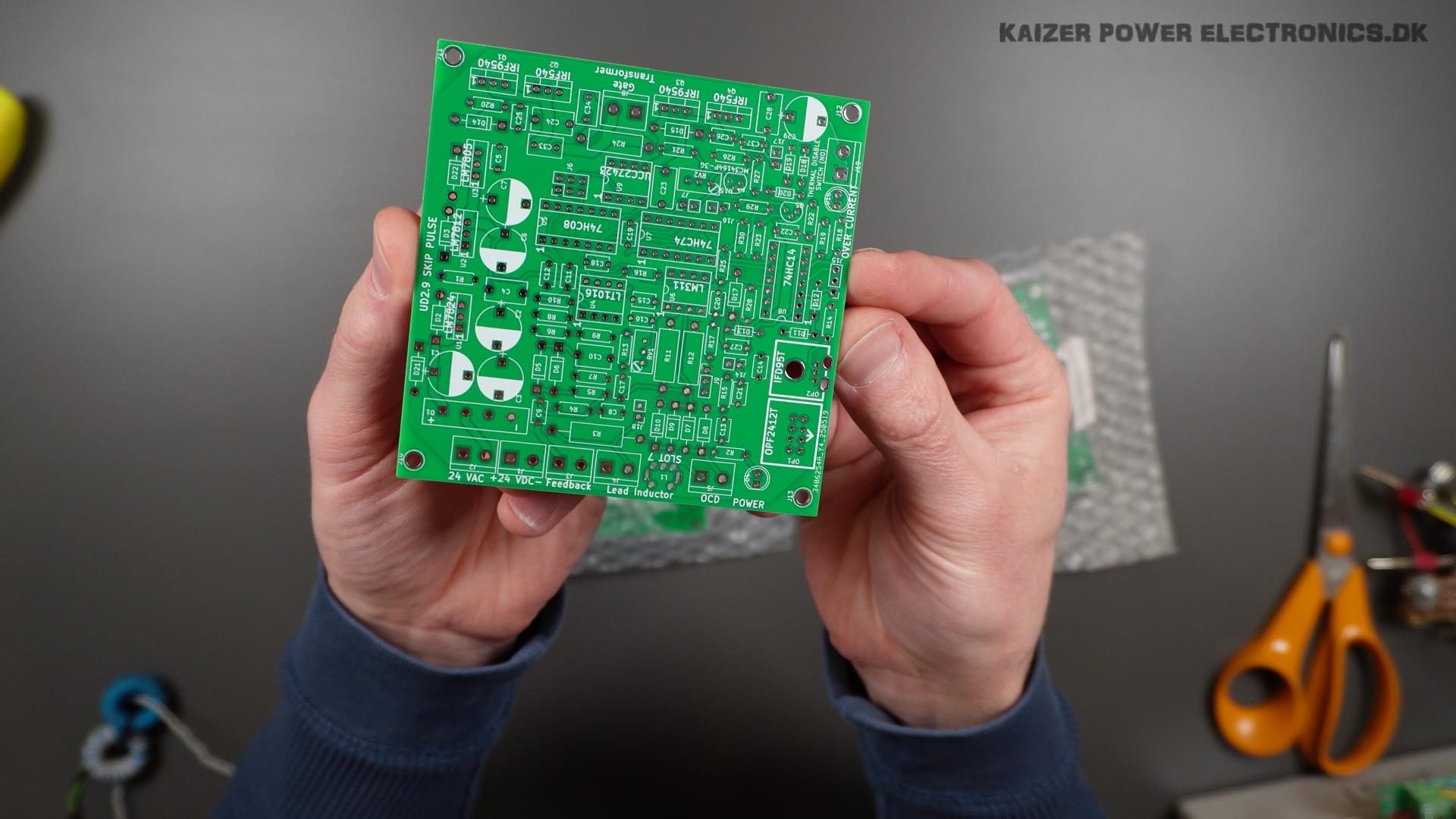
The drivers and interrupters printed circuit boards were ordered from a PCB manufacturer, by using the free gerber files in the DRSSTC PCB package. Quality is very good. Silkscreen has no errors or missing prints. Feed-through sticking between layers is perfect as well.
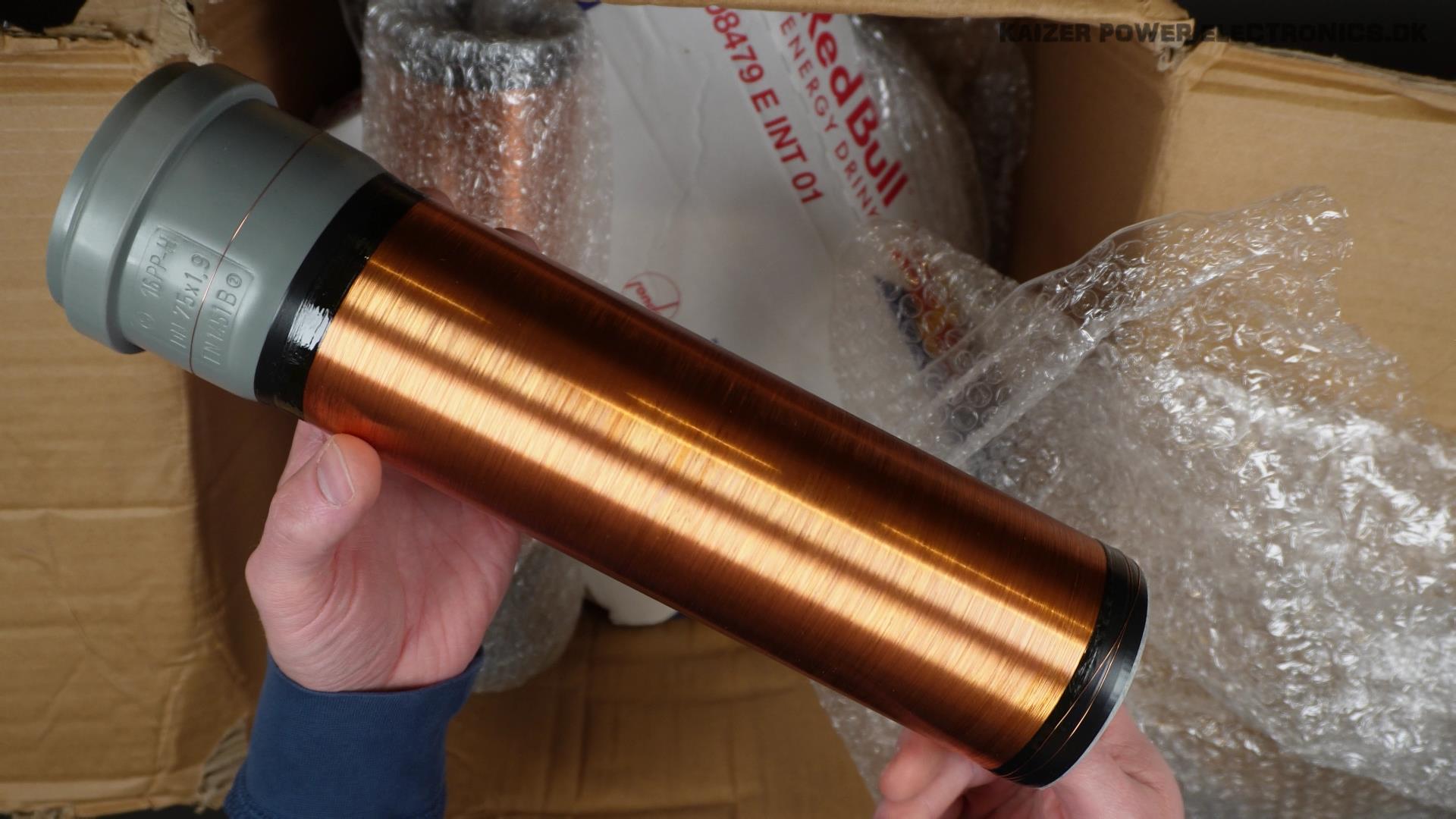
The secondary coils do feel a bit thin, with only two layers of thin varnish. It is not a thick layer of heavy flowing polyurethane, feels like its spray on varnish. The wire is secured in both ends with electrical tape, which makes no difference for operation, but does not look great. I did not try out the mounting set and topload holder yet.
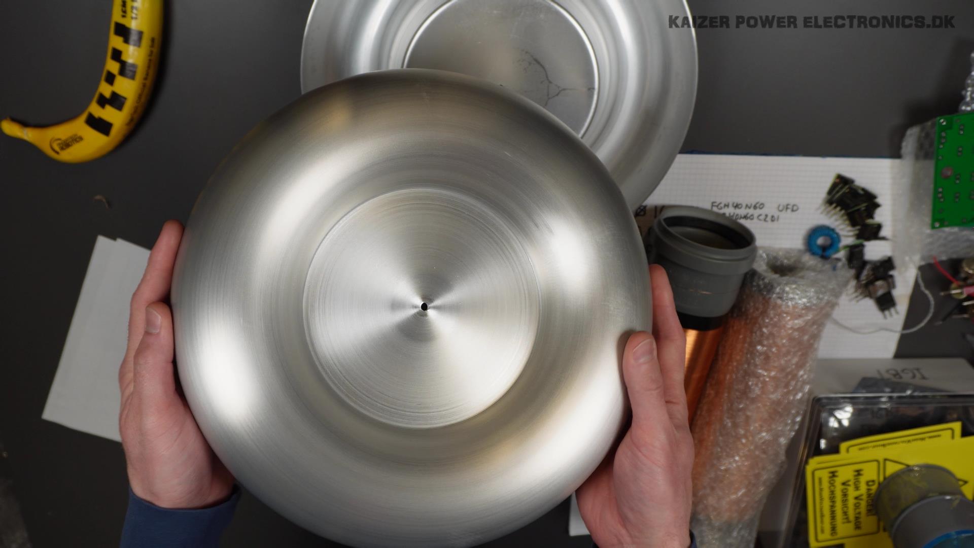
The toploads are very high quality! Very thick material, so very sturdy and resistant to bumps and dents. There is however only the center hole to make it completely round, it can easily skew a bit if a too small screw is used, or the two parts are pushed opposite directions.
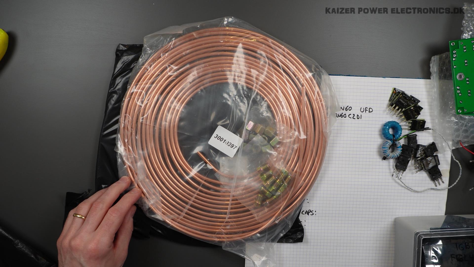
For the primary coil, the brake line copper tube is perfect for this sized Tesla coil. Its 3/16″ diameter (4.76 mm) has all the advantages of the large copper tubing, like being hollow, so skin effect is much smaller, than if we used solid wire. Normally solid wire would easily be used in a coil of this size.
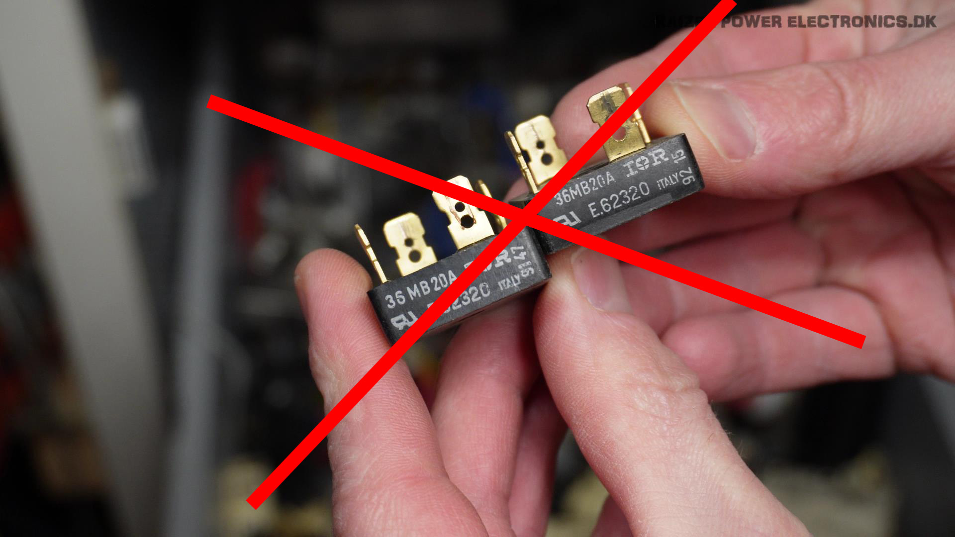
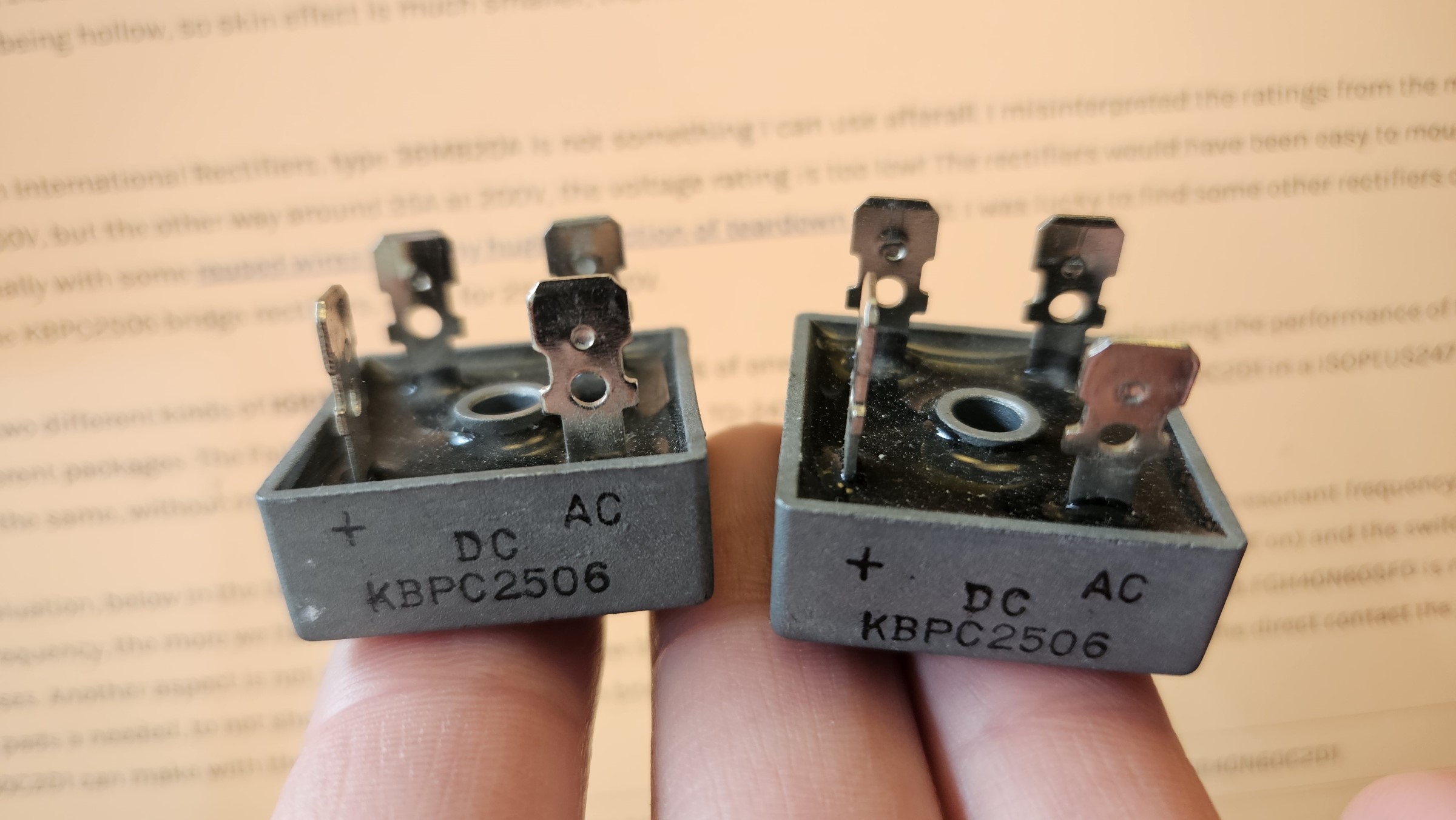
The rectifiers from International Rectifiers, type 36MB20A is not something I can use afterall. I misinterpreted the ratings from the model name, it was not 20A at 350V, but the other way around 35A at 200V, the voltage rating is too low! The rectifiers would have been easy to mount with cable shoe legs, especially with some reused wires from my huge collection of teardown wires :D. I was lucky to find some other rectifiers of the same package type, the KBPC2506 bridge rectifiers, rated for 25A at 600V.
I chose to use two different kinds of IGBTs, mostly due to not having 16 of one kind. This is perfect for evaluating the performance of the “same” rated die in two different packages. The Fairchild FGH40N60SFD comes in a TO-247 package and the Ixys IXGR40N60C2D1 in a ISOPLUS247 package, which is essentially the same, without mounting hole.
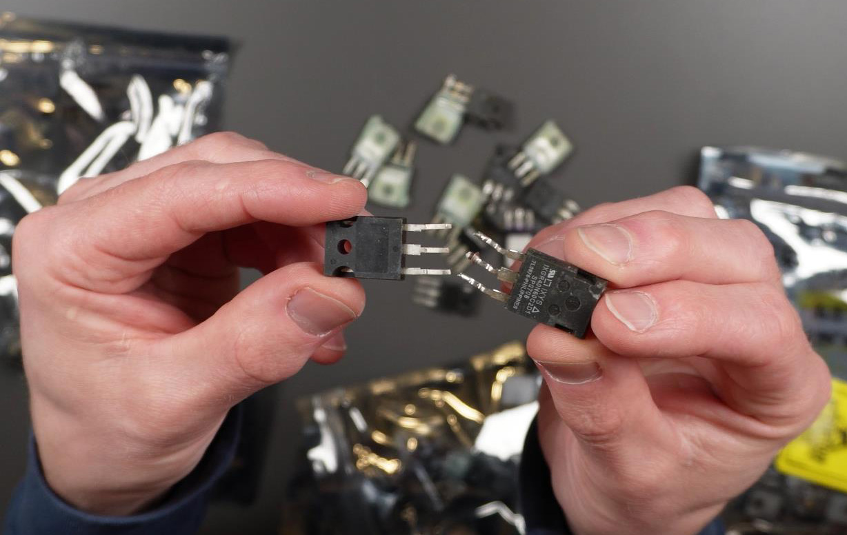
From the evaluation, below in the table, my verdict is that the Ixys IXGR40N60C2D1 is better suited for a 300 kHz resonant frequency. The higher switching frequency, the more we have to pay attention to gate charge (how much energy we need to drive the IGBT on) and the switching speeds/losses. Another aspect is not just losses, but also how to dissipate that energy. The flange of the Fairchild FGH40N60SFD is not isolated, so insulating pads a needed, to not short circuit the legs of the bridge. This makes power dissipation worse than the direct contact the Ixys IXGR40N60C2D1 can make with the heat sink.
| Fairchild FGH40N60SFD | Ixys IXGR40N60C2D1 | |
| Flange | Collector potential | Isolated |
| Saturation Voltage VCE(sat) | 2.3 V | 2.7 V |
| Pulsed Current ICM @ 25 oC | 120 A | 200 A |
| Maximum Power Dissipation PD @ 25 oC | 290 W | 170 W |
| Gate Charge QC | 120 nC | 95 nC |
| Turn-On Time td(on) | 24 ns | 18 ns |
| Rise Time tr | 43 ns | 20 ns |
| Turn-Off Time td(off) | 120 ns | 130 ns |
| Fall Time tf | 30 ns | 80 ns |
| Turn-on Switching Losses | 1.14 mJ | 0.6 mJ |
| Turn-off Switching Losses | 0.48 mJ | 0.5 mJ |
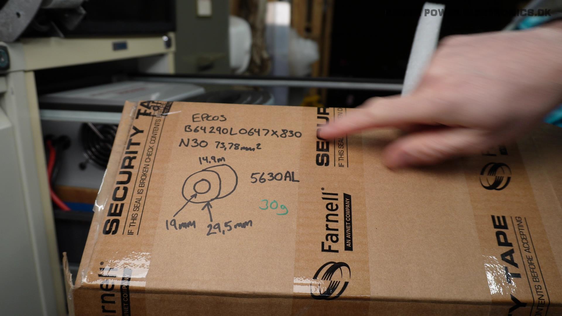
For the current transformers (CT) and gate drive transformers (GDT) the same type and size ring cores can usually be used. I chose a Epcos B64290L0647X830 which is made from N30 material with a 5630 AL value. Most cores / materials with a AL value around 5000 is suitable.
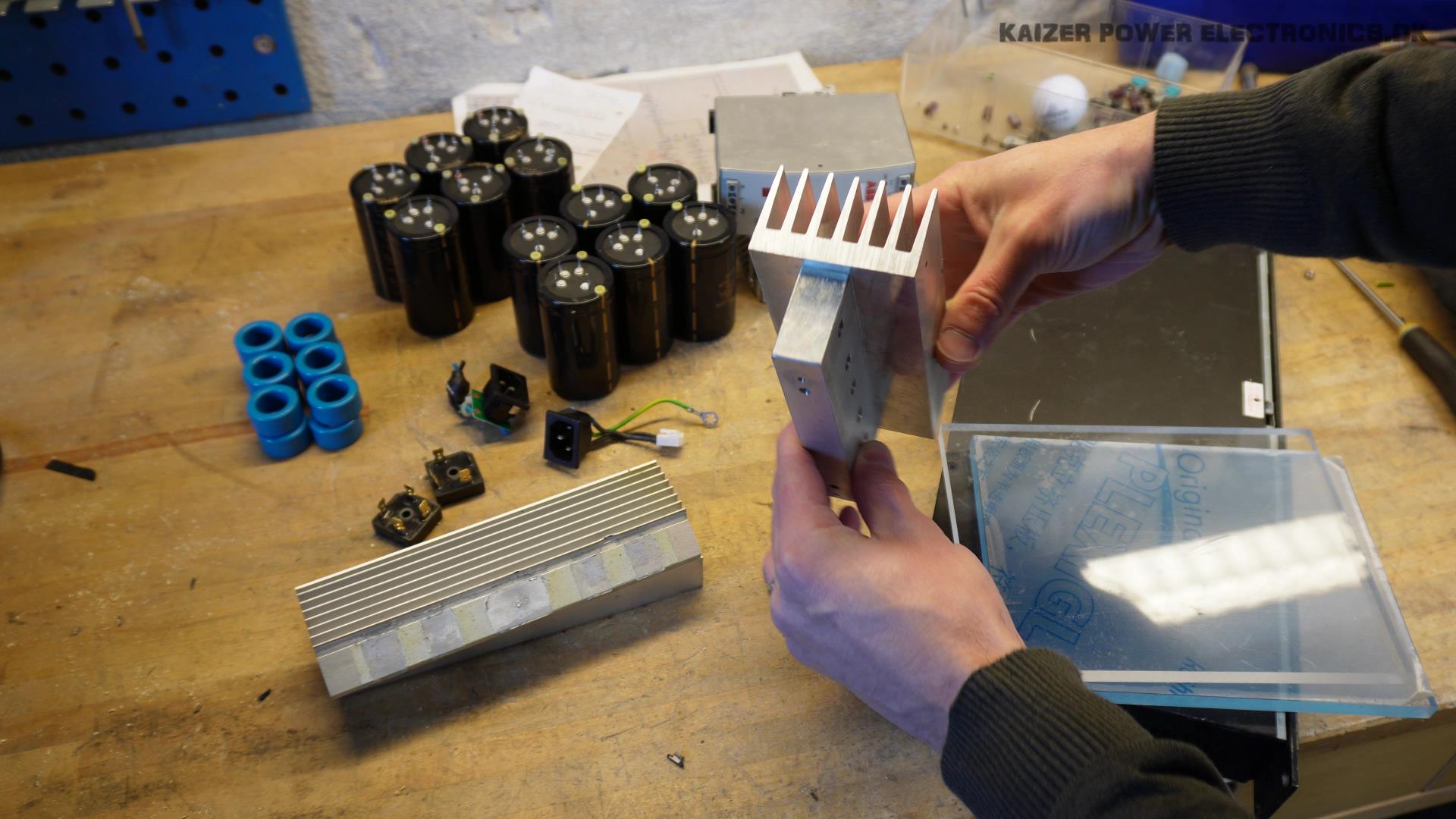
The heat sinks is two different types. I think that the flat heat sink for the ISOPLUS247 package is the original heat sink from the Ixys IXGR40N60C2D1 that was used in a induction stove / cooker. The other type is in two parts, a block for the IGBT mounting and a part with fins to go on top of that.
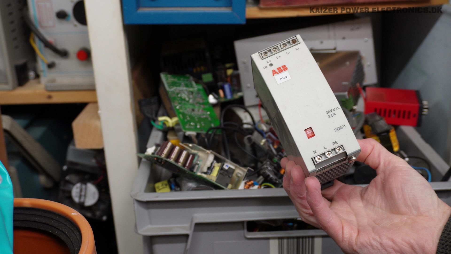
The power supply for the driver, I chose a ABB SD821, 24 VDC at 2.5 A industrial power supply, with 230 VAC input. It just takes up less space than a transformer (also I did not have any suitable transformers), and I can skip having the rectifier / capacitors on the driver board itself.
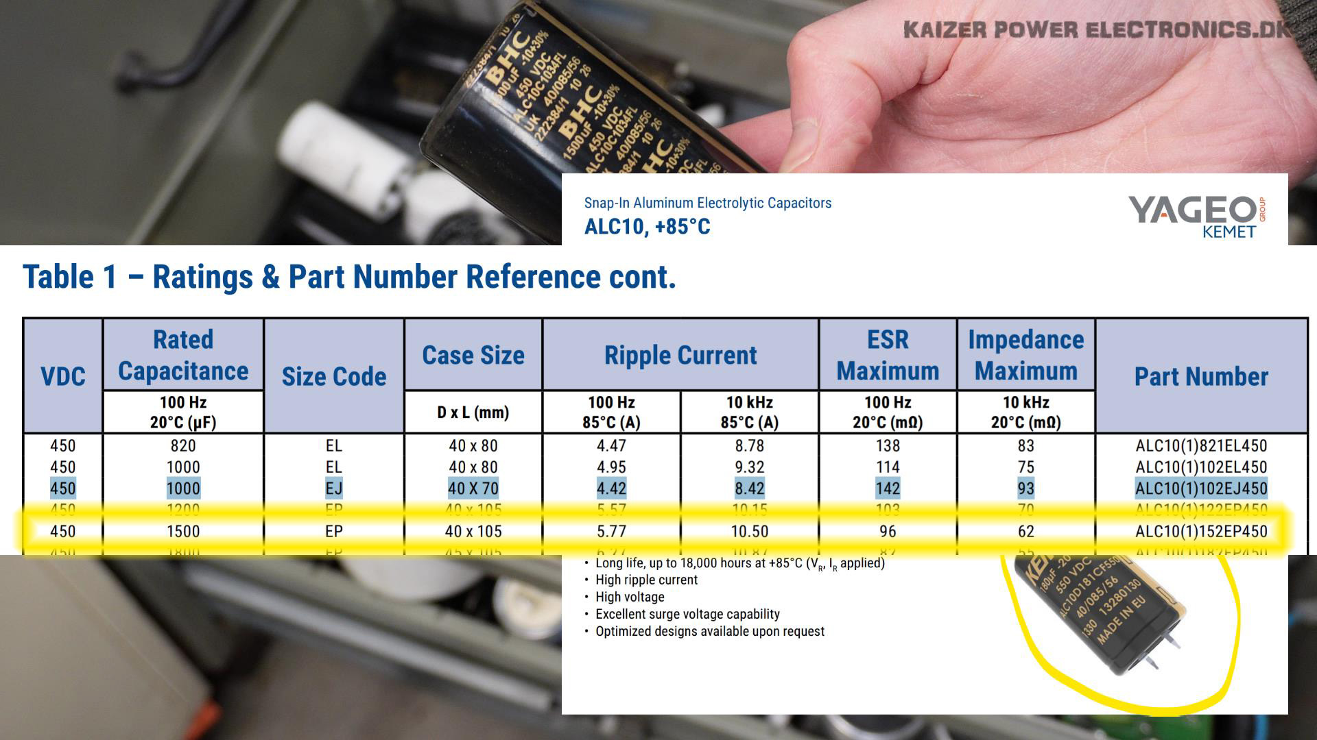
6x 1500 uF Epcos ALC10 electrolytic capacitors in parallel, is used to make a 9000 uF at 450 VDC bank for the DC bus capacitance. It is able to deliver high peak currents from the 6 capacitors in parallel and withstand around 60 A ripple current.
Building
13th April 2026 to 15th May 2026 was spend on making circuit boards, populating printed circuit boards, construct all mechanical parts and prepare terminations for the final electrical connection between parts.
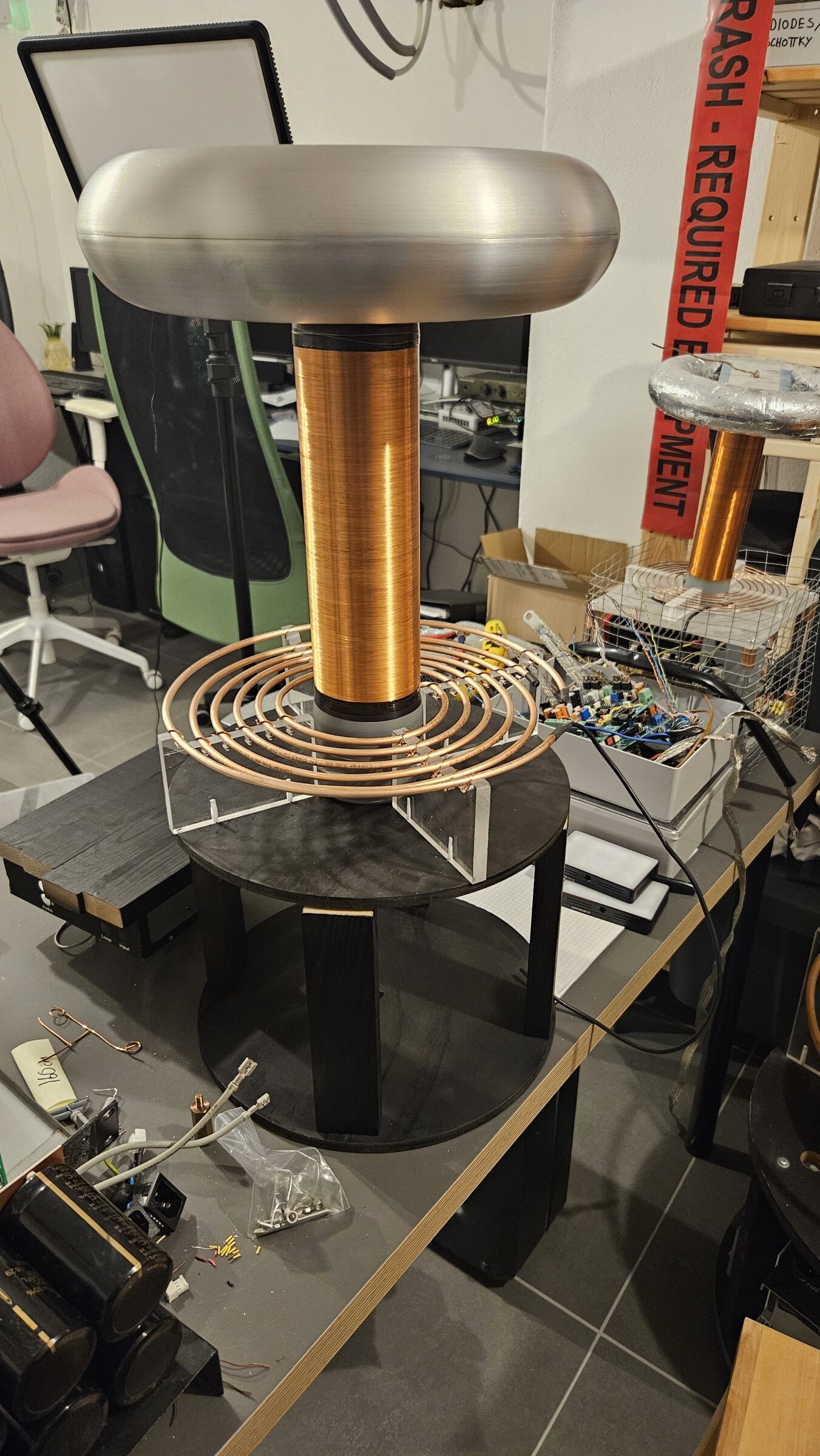
I value good craftmanship and simpleness, 3D printers and laser cutters are not basic needs for DIY. The amount and complexity of tools used, is kept to a minimum:
- Drill press
- Hand drill
- Tapping set
- Wood saw
- Hack saw
- Wise
- Hammer
- Overhead router
- Soldering iron
The enclosure is made from two 8mm plywood discs, 30 cm in diameter and with four 20 cm wooden standoffs between them. The weight of the primary coil, MMC, secondary coil and topload, does not dictate that a more sturdy construction should be needed.
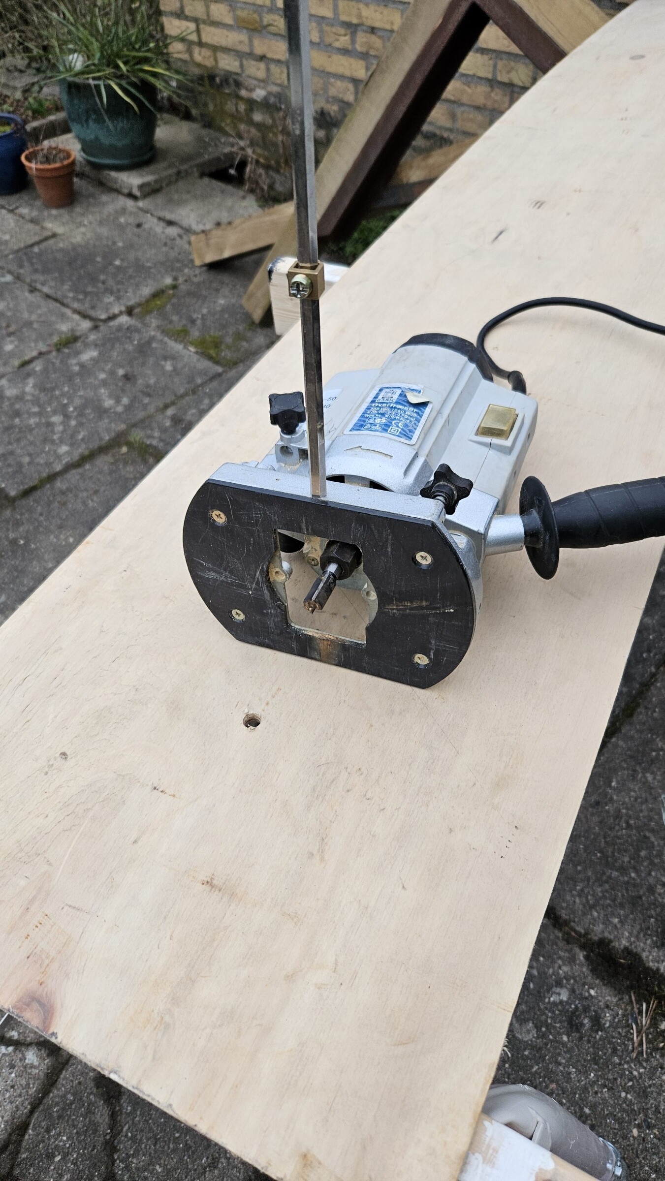
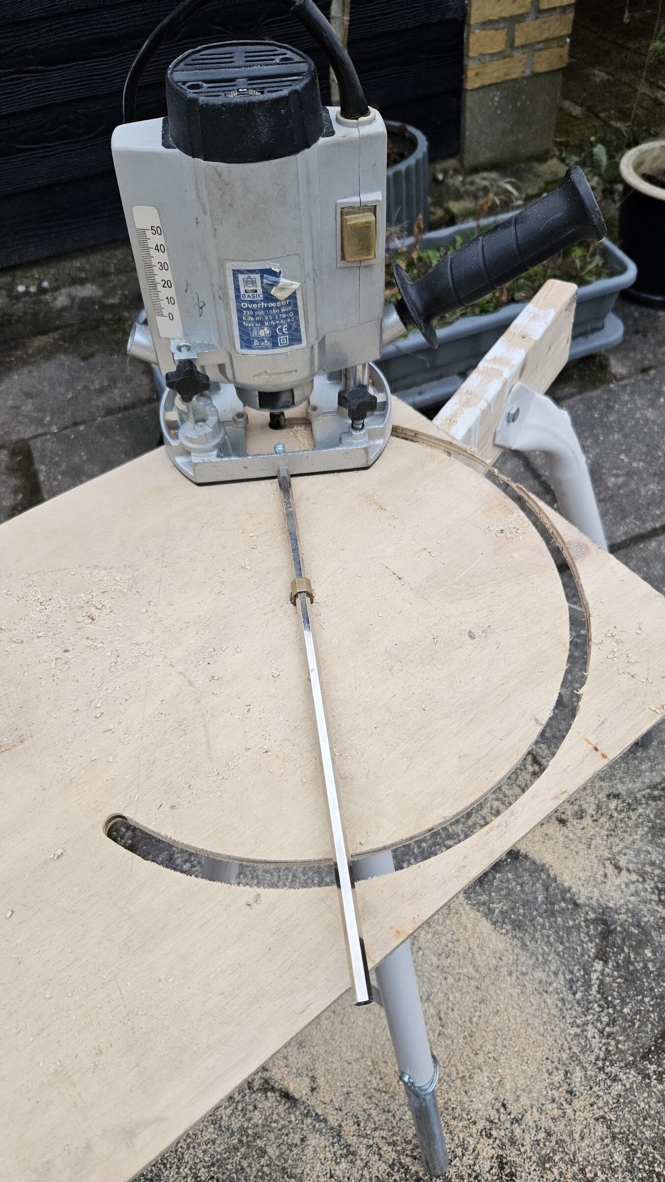
The 30 cm plywood discs are easily made with a modified overhead router. A metal rod is drilled into the side of the router frame, with an adjustable clamp nut on it. The clamp nut originates from the terminal of a large electrical contactor. The screw of the clamp nut is used as the center of the needed circle cut and its position on the metal rod is the radius of the circle, to the edge of the overhead routers tool insert.
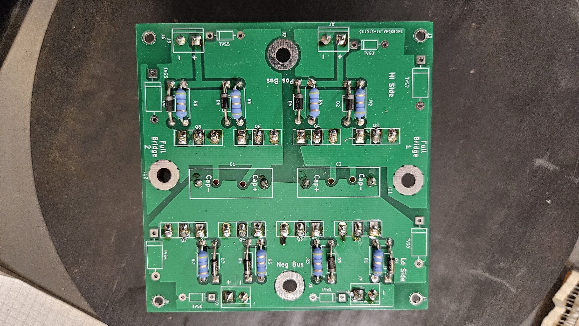
The power electronics full-bridge PCB is not populated with TVS diodes, as I find it overkill. There is examples of TVS diodes across C-E junction of an IGBT that can cause breakdown failure, that would otherwise just be mitigated by the snupper capacitors. I originally planned for a single 2.2uF snubber capacitor, but due to space constraints is limited to one 0.47uF and one 0.1uF snubber capacitors. Testing and measurements will be used to verify if it is sufficient.
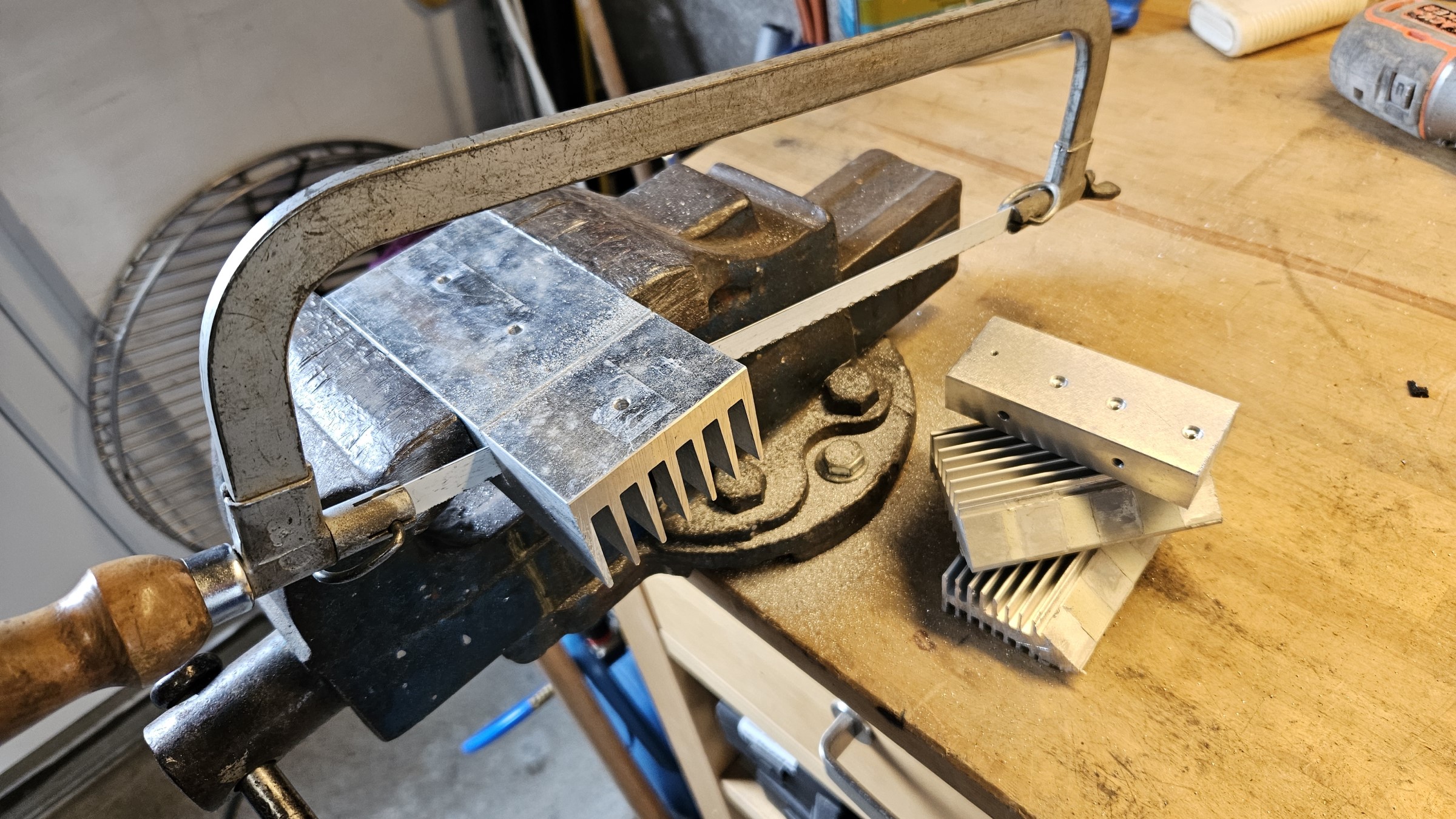
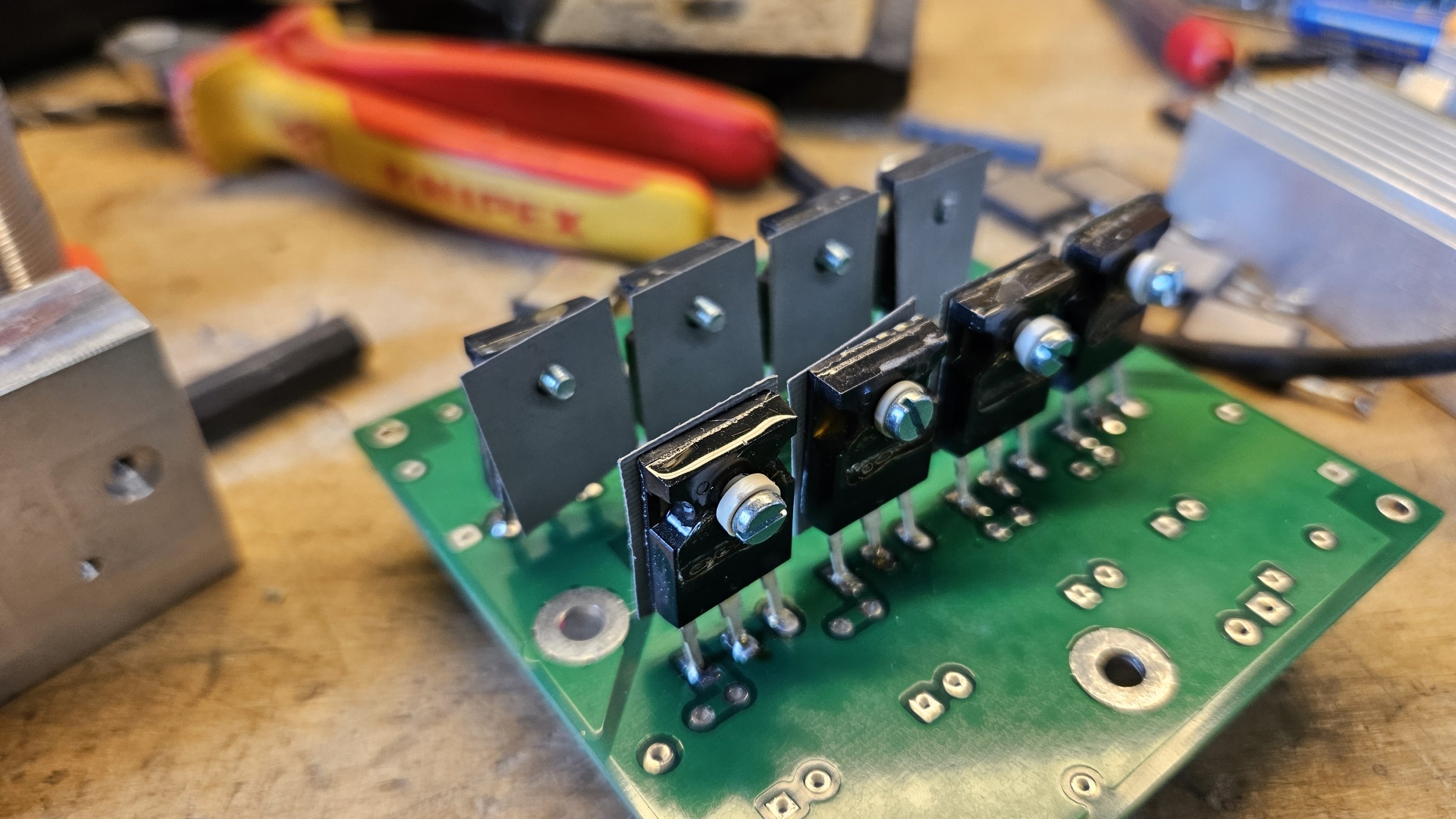
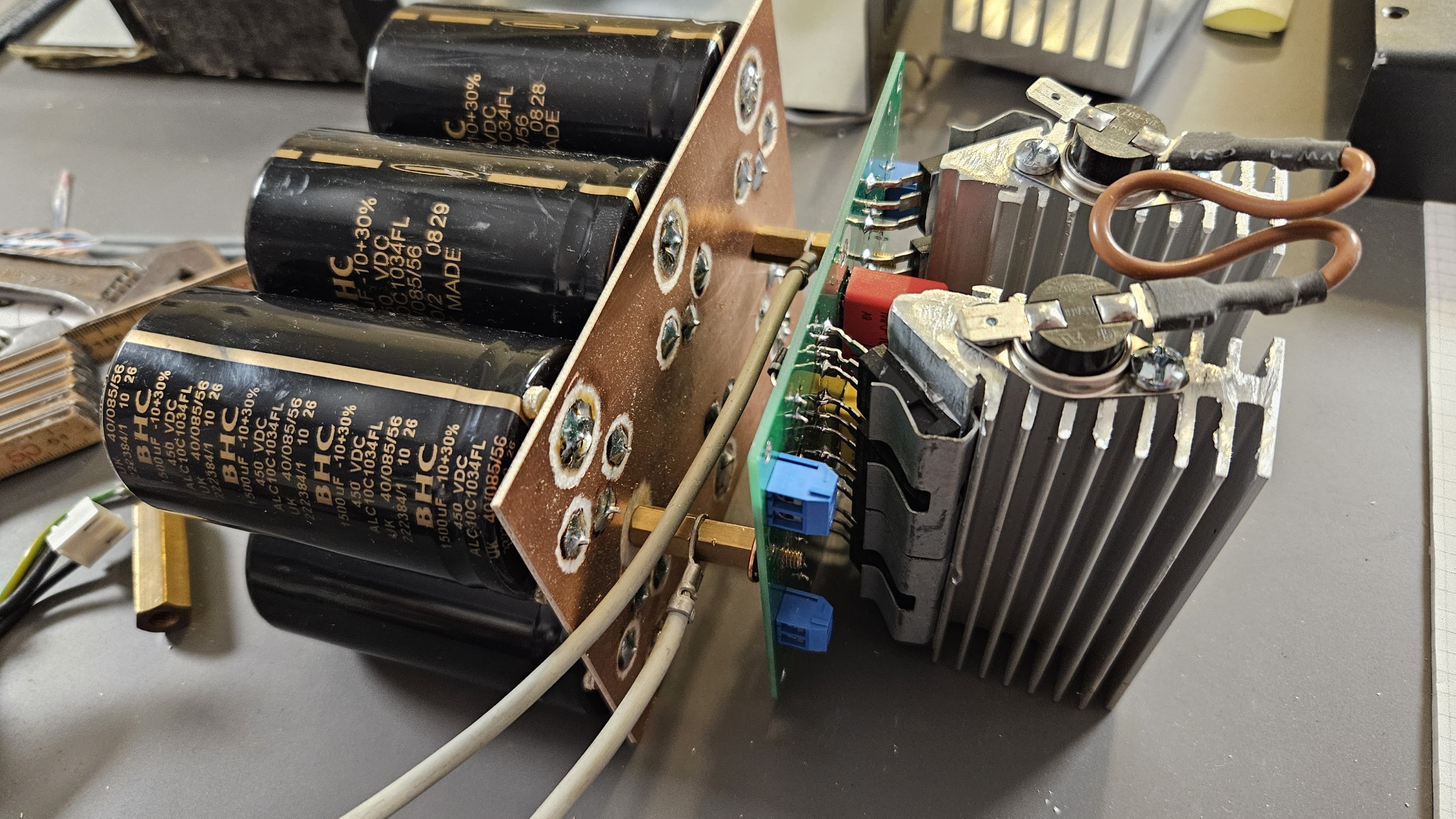
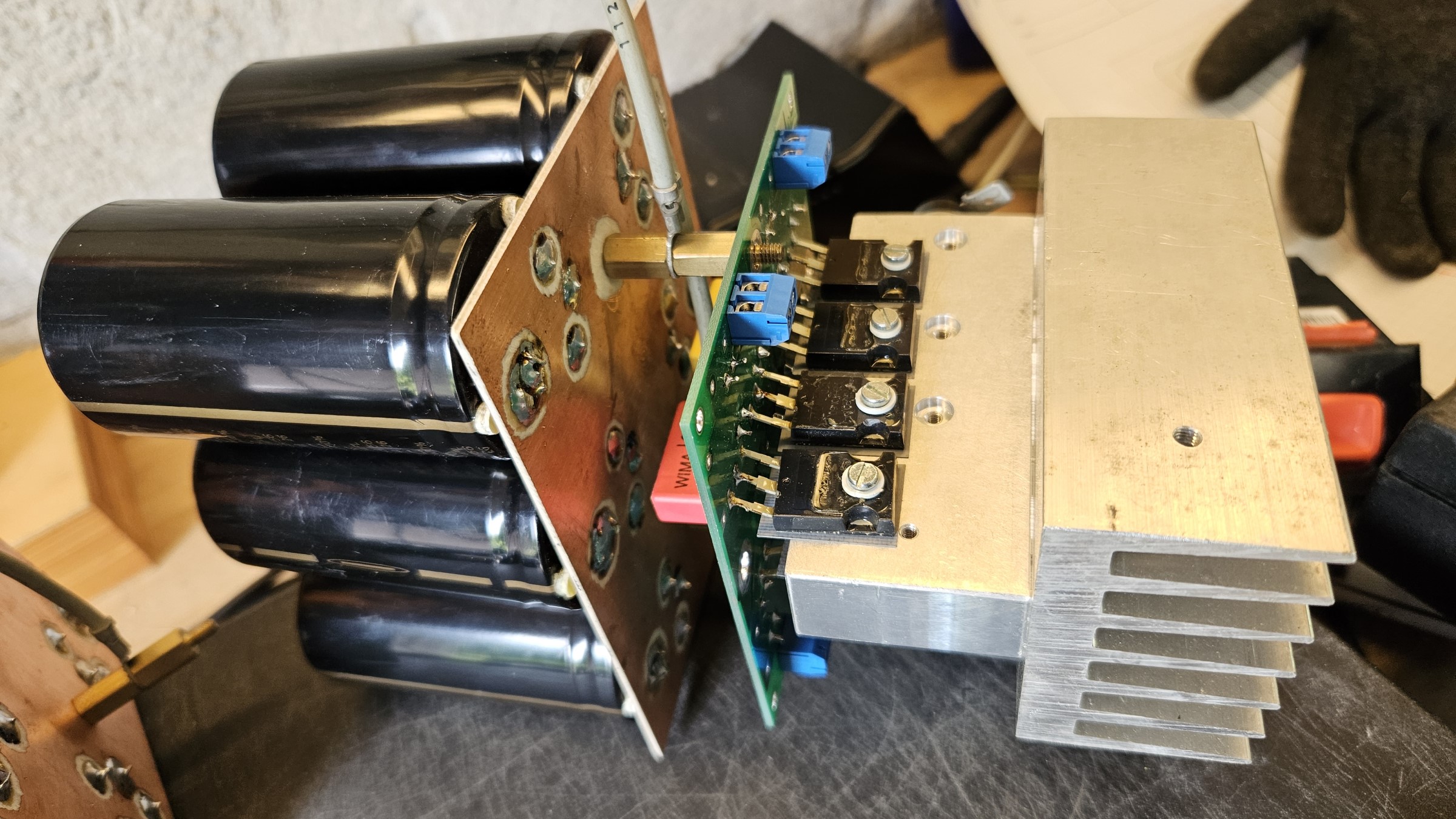
Two different heat sink solutions is tested. One type (Fairchild FGH40N60SFD) with screw holes and another type (Ixys IXGR40N60C2D1) with spring loaded clamp-on. IGBTs with screw hole is normally not with an isolated tab, so pads are used to avoid short-circuiting the entire bridge. Adding pads makes for a worse heat transfer, a alternative solution could be to cut the heat sink into four pieces, isolated from each other, they would however be floating at IGBT collector potential. The clamp-on IGBT in this case, is with isolated tap and therefore has superior heat transfer properties over the latter.
For the primary coil I chose to use 10mm thick acrylic for the primary holders, because I already had it in stock from making the DRSSTC 1! I chose to use 4 holders, by drilling 5mm holes spaced 10 mm apart, that pattern can just be shifted by 2.5 mm per holder and you get the pattern of a flawless spiral. A strike rail is added on the primary coil holder, slightly elevated in regard to the primary coil. All mounting to the base plate is done with nylon screws, to avoid metal being too near to the primary coil.
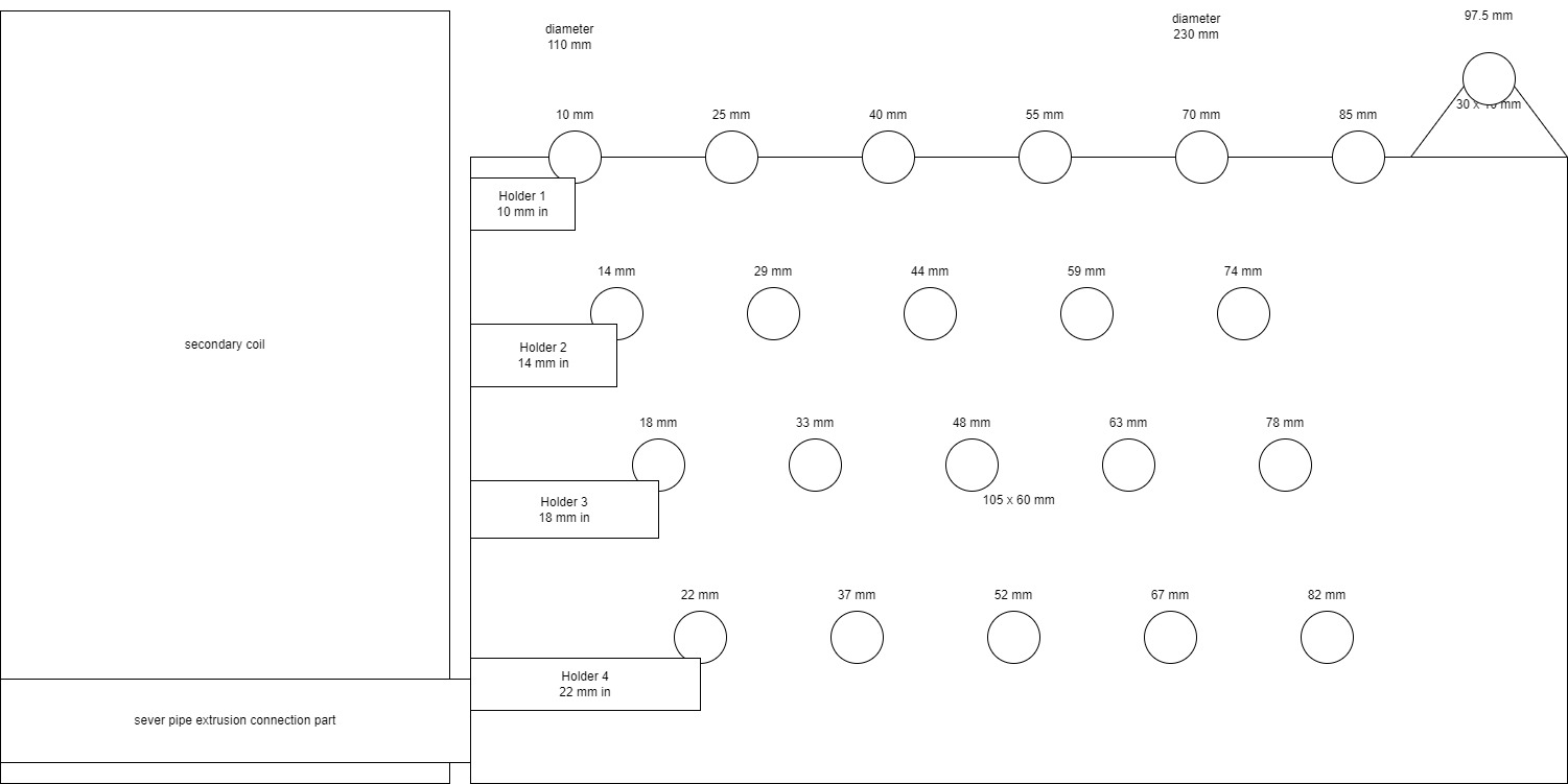
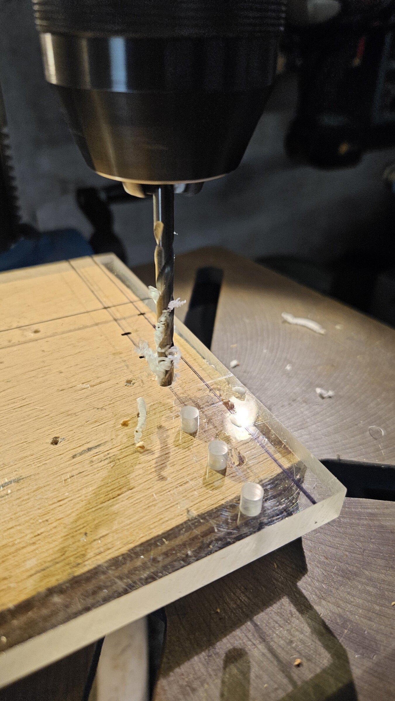
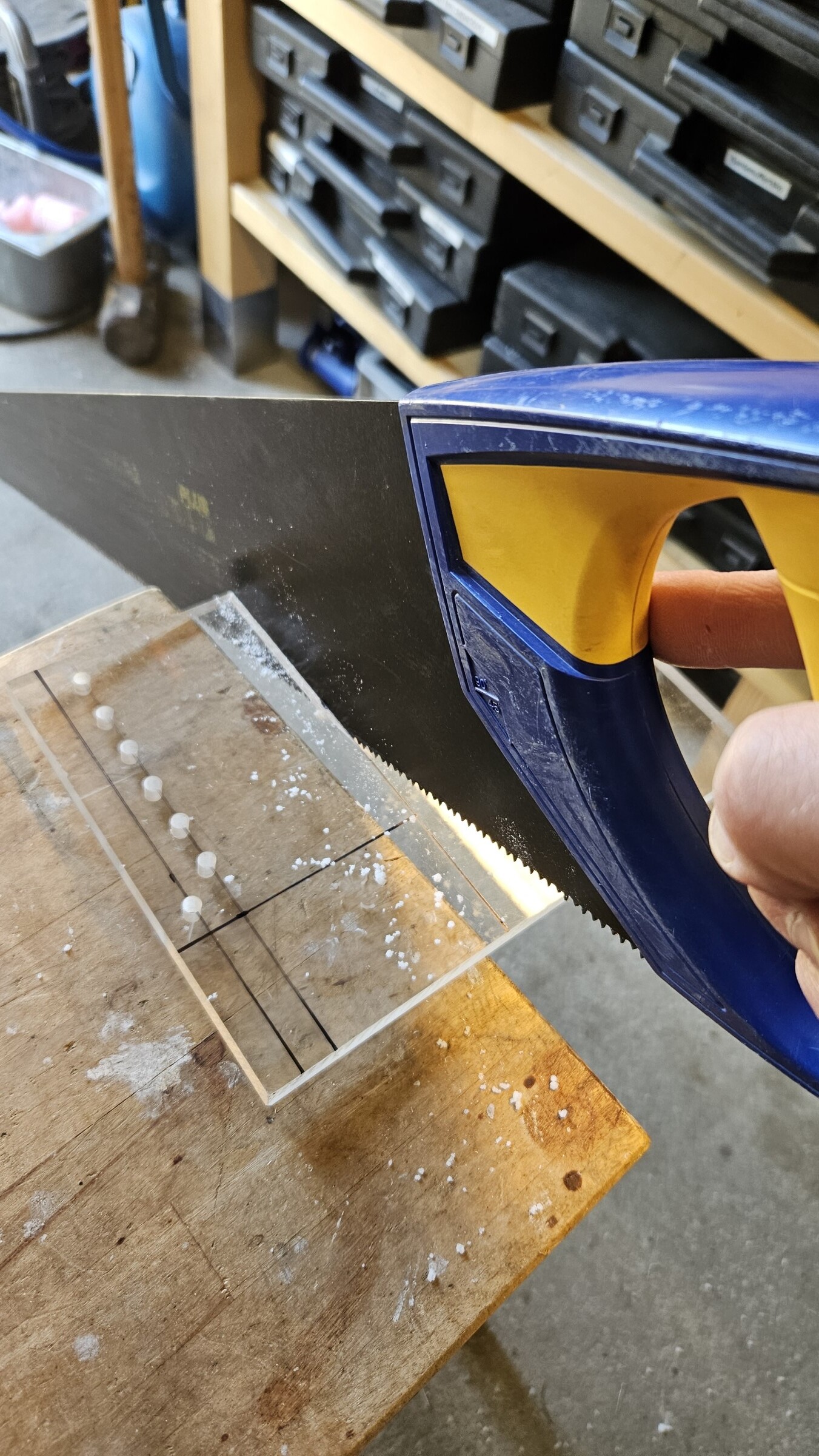
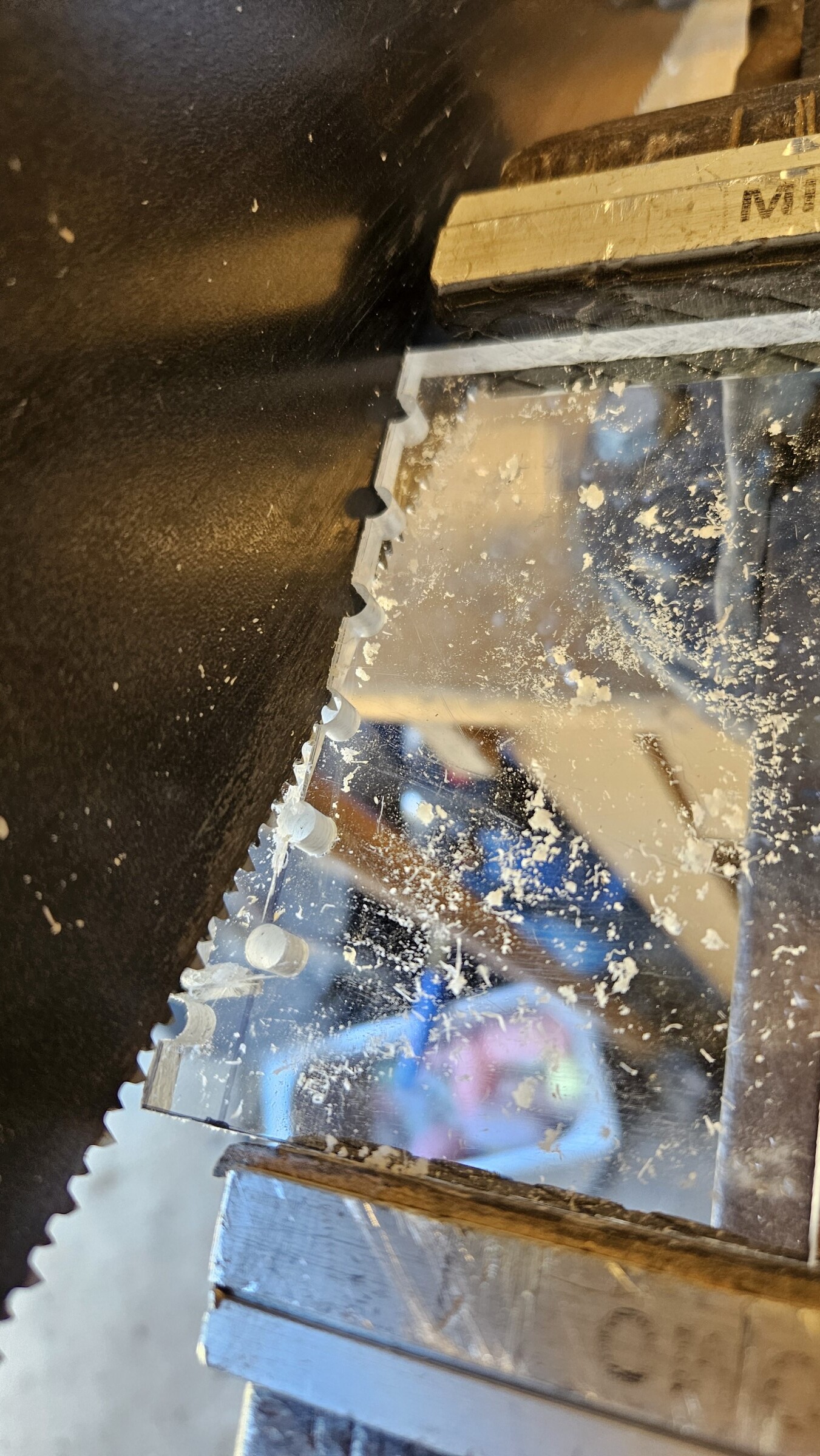
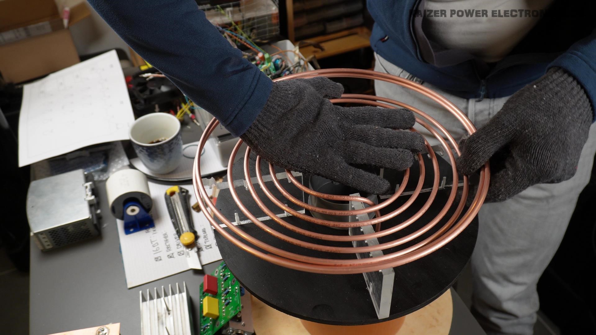
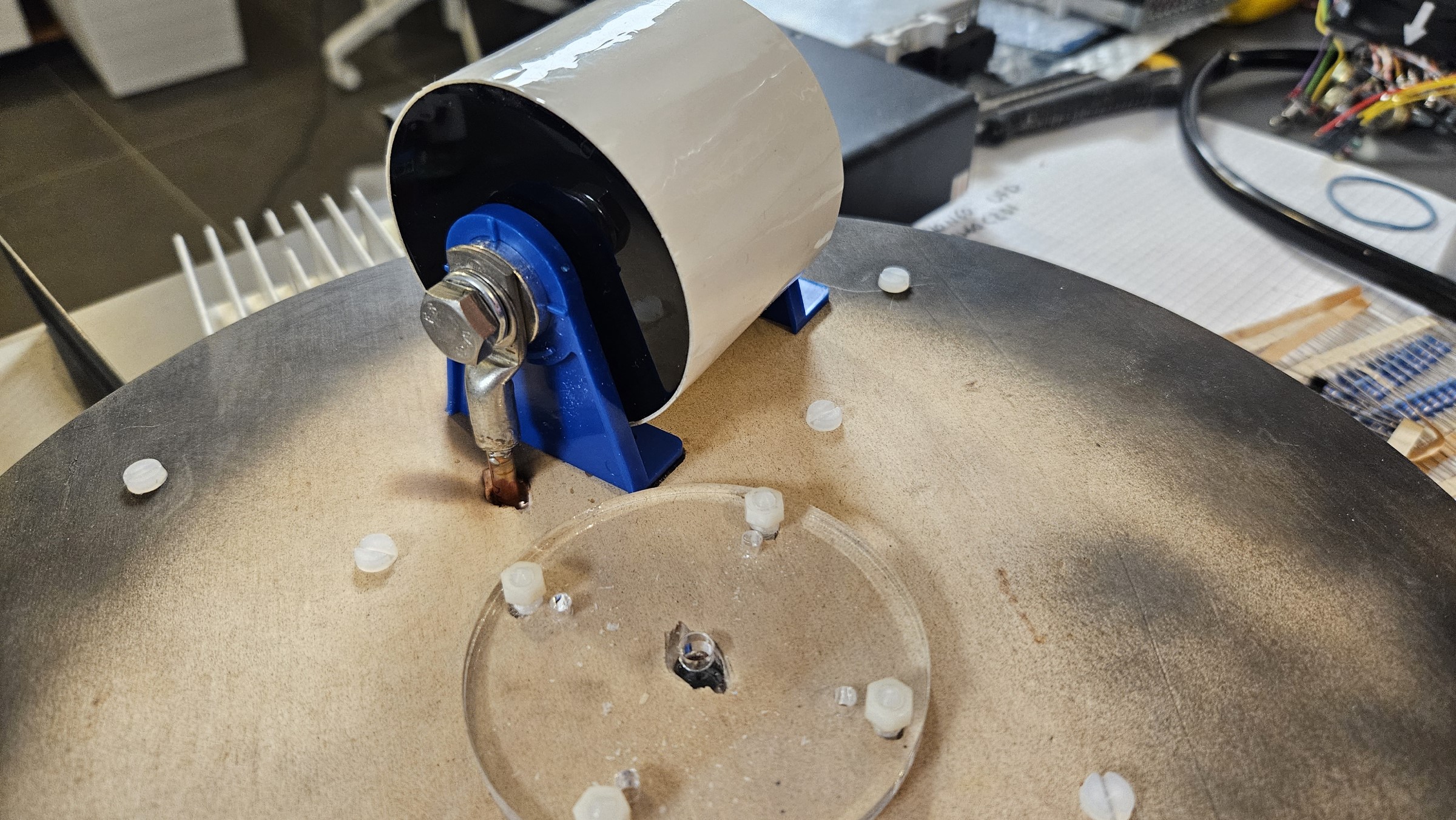
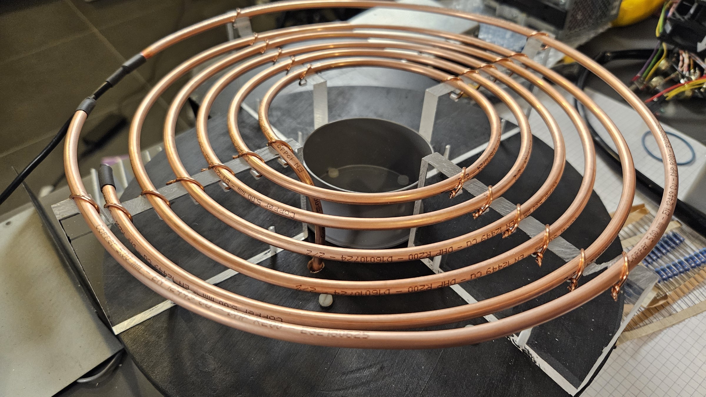
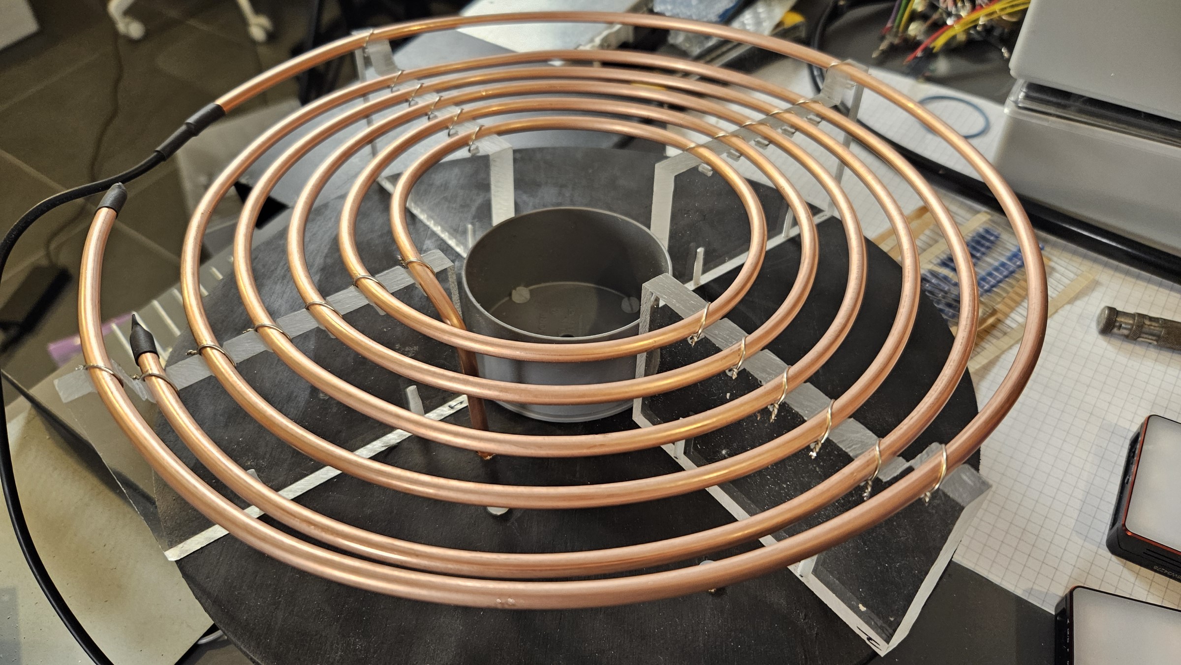
The secondary coil is winded on a regular gray PVC sewer pipe and the supplied mounting set, uses an end cap from the same system. This end cap can only be used with the full pibe head and gasket. This either dictates a more complex platform construction or just go with the taller primary holders.
The mounting set did not include anything for the top of the secondary coil. I cut a piece from another 75 mm sewer pipe, cut a slot in it and glue it in place inside. A 73 mm diameter hole saw was used to make a disc that has a perfect fit, to rest on the slotted pipe piece on the inside. All glued together and only using nylon screws for the topload connection.
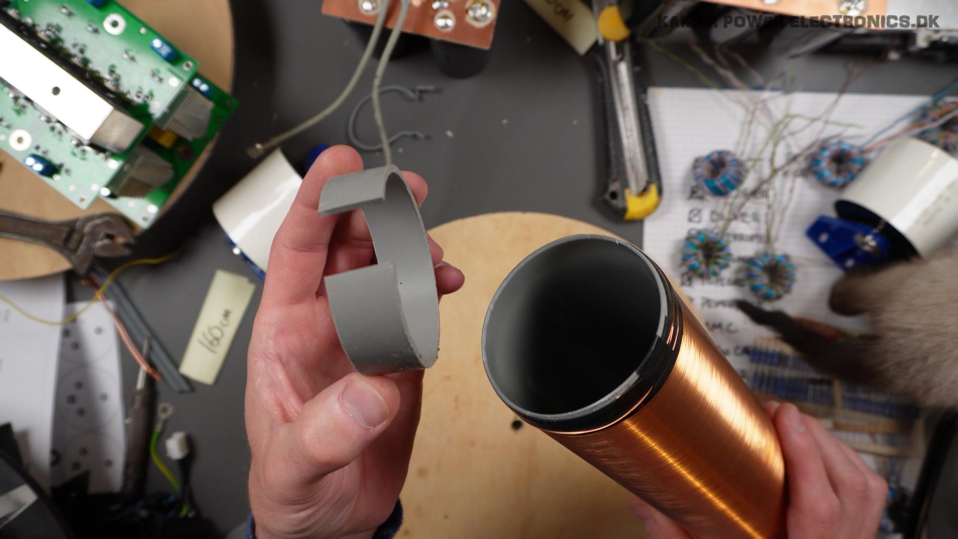
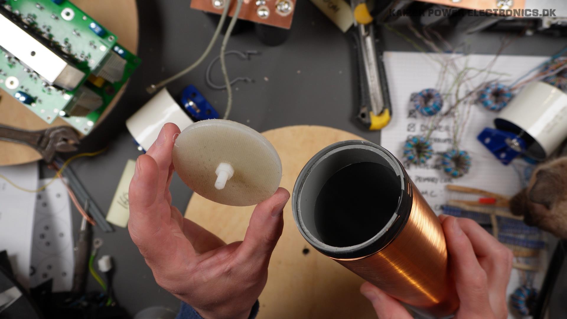
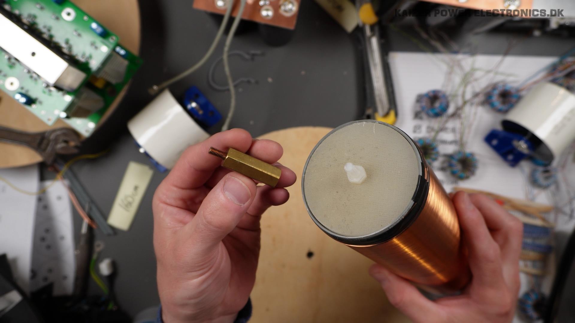
No metal on the inside of a secondary coil! This will help prevent internal flashovers inside the secondary coil.
The topload mounting hardware is replaced with a brass standoff, that provide a good mechanical and sturdy connection from the nylon bolt and ensures a good low resistance connection from secondary coil to topload. The secondary wire will be protected from direct wear of the toploads weight and jigglyness.
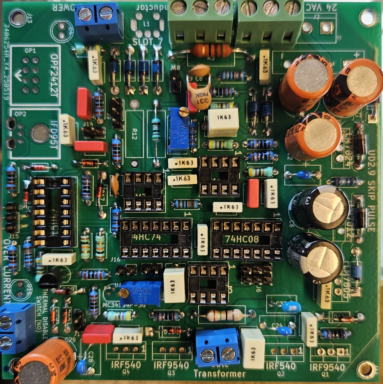
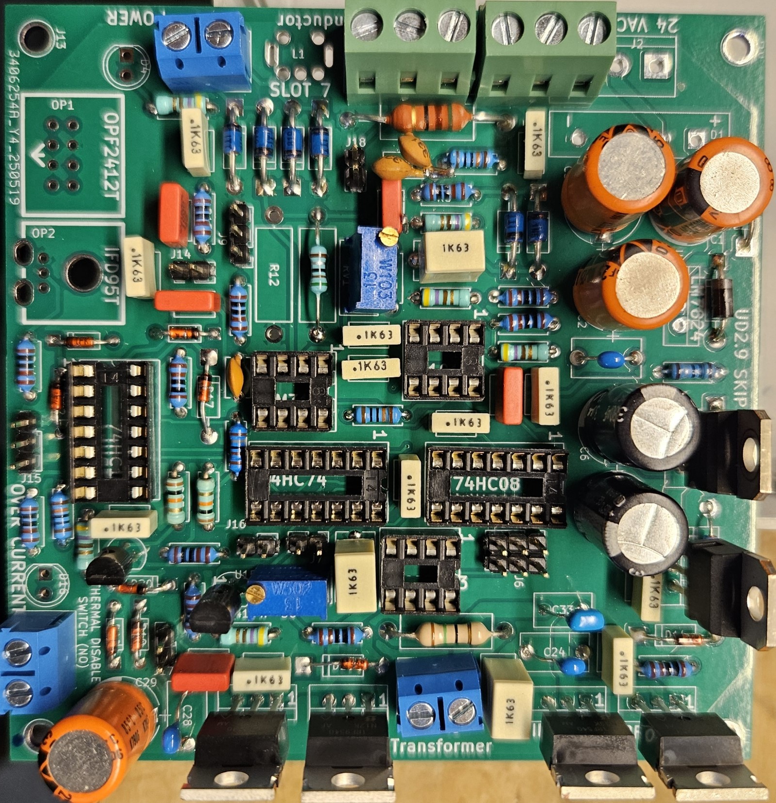
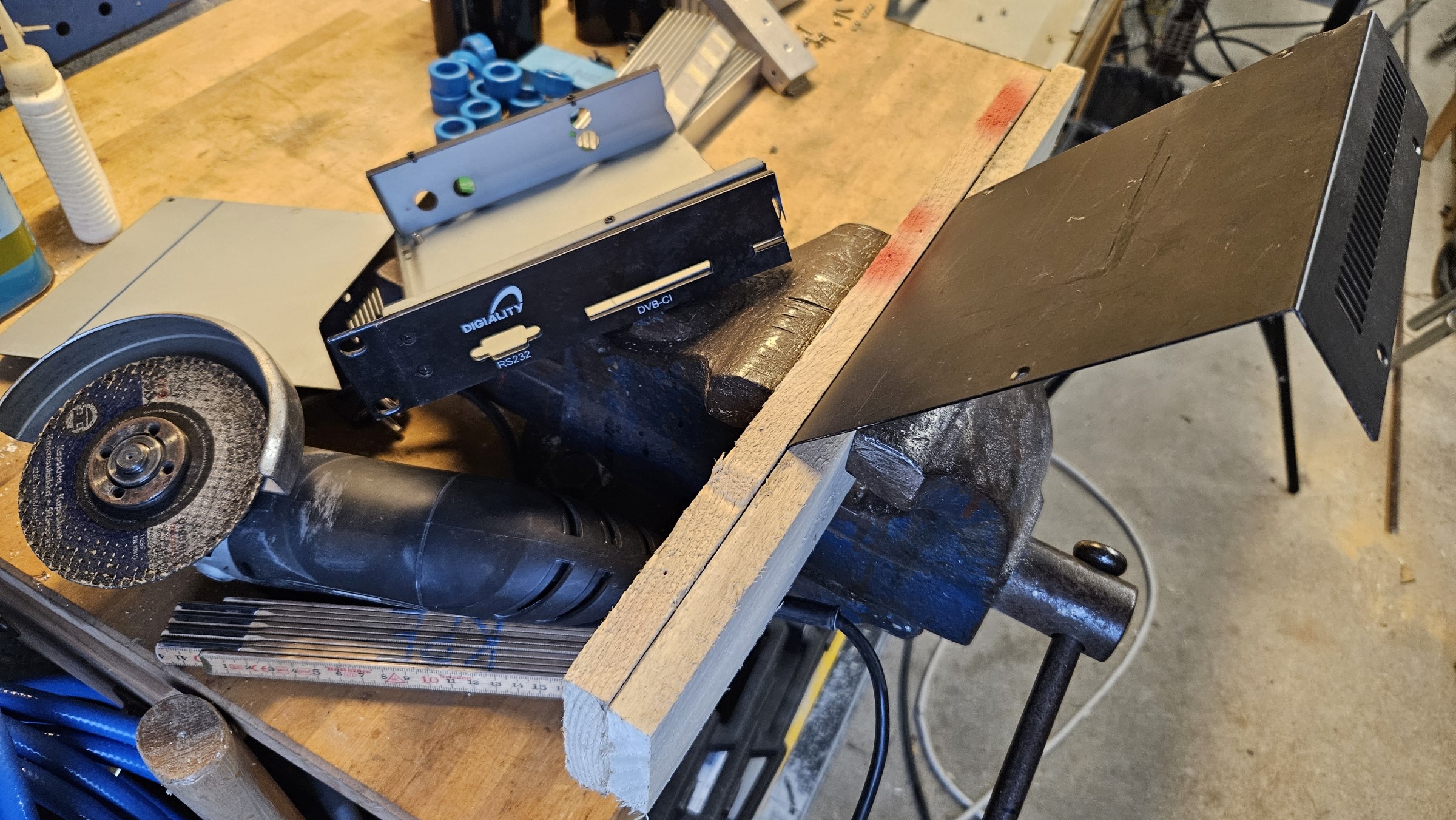
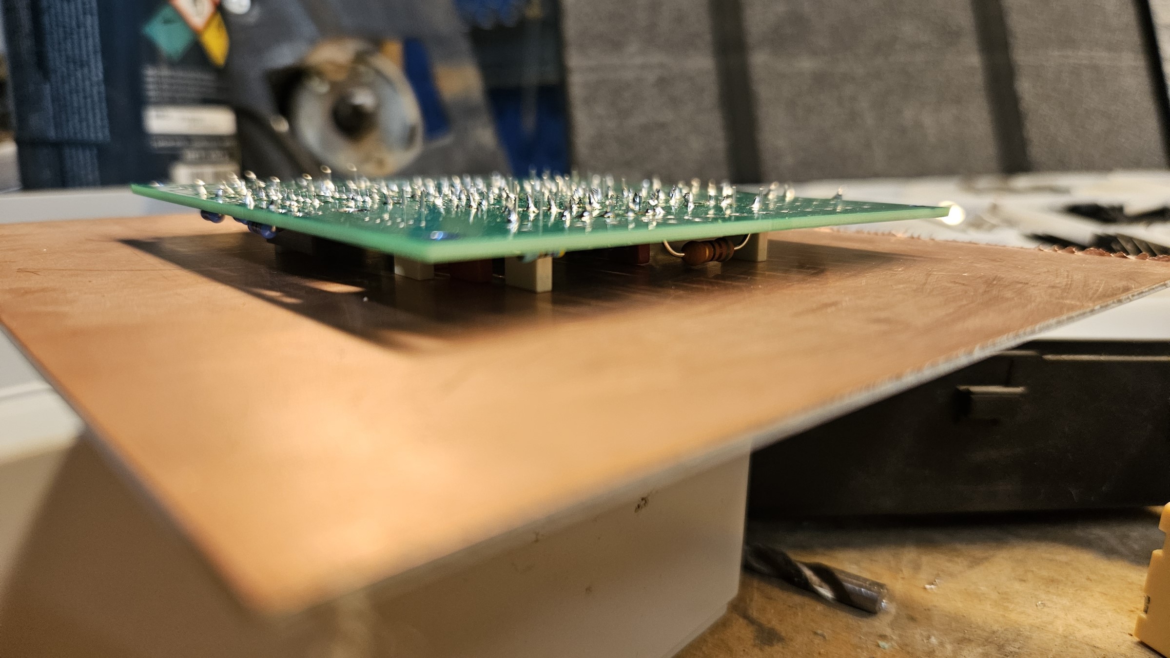
The driver used it the DRSSTC Universal Driver 2.9 (UD2.9 by prof9dc). When soldering through-hole components to a printed circuit board, bending the legs to avoid components falling out or displacing, is a common practice. Bent legs is however also a nuisance, if you have to change a defective part or do fault finding. I have solved this issue by soldering in components based on their height. By going from lowest to tallest component, I can populate the board, cover the components with a plate, turn it all up-side-down and easily solder all the components without them falling out. The sequence used for this printed circuit board was:
- Resistors and diodes
- IC sockets
- Small film capacitors
- Large film capacitors
- Terminals
- Electrolytic capacitors
- Transistors and voltage regulators
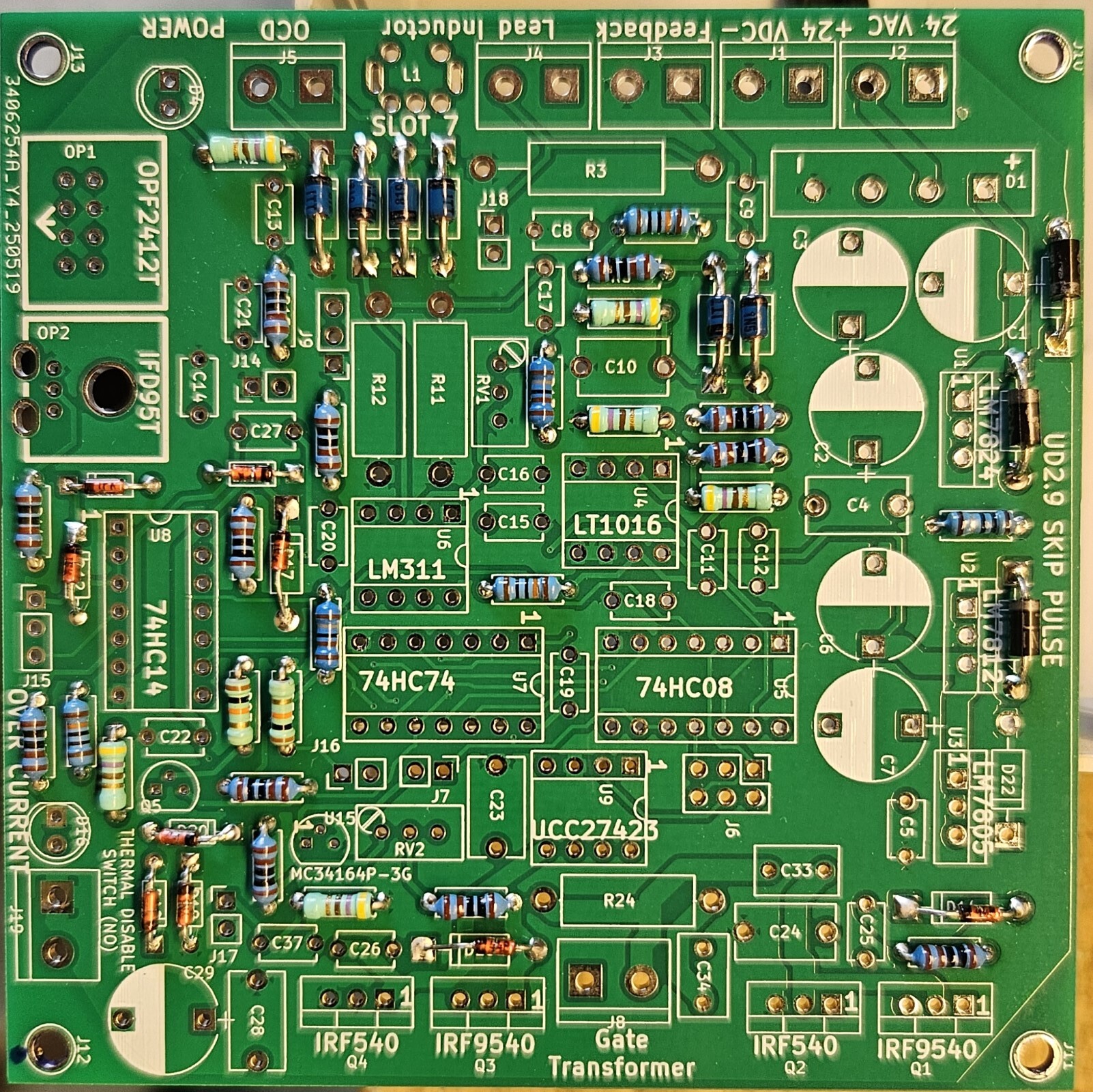
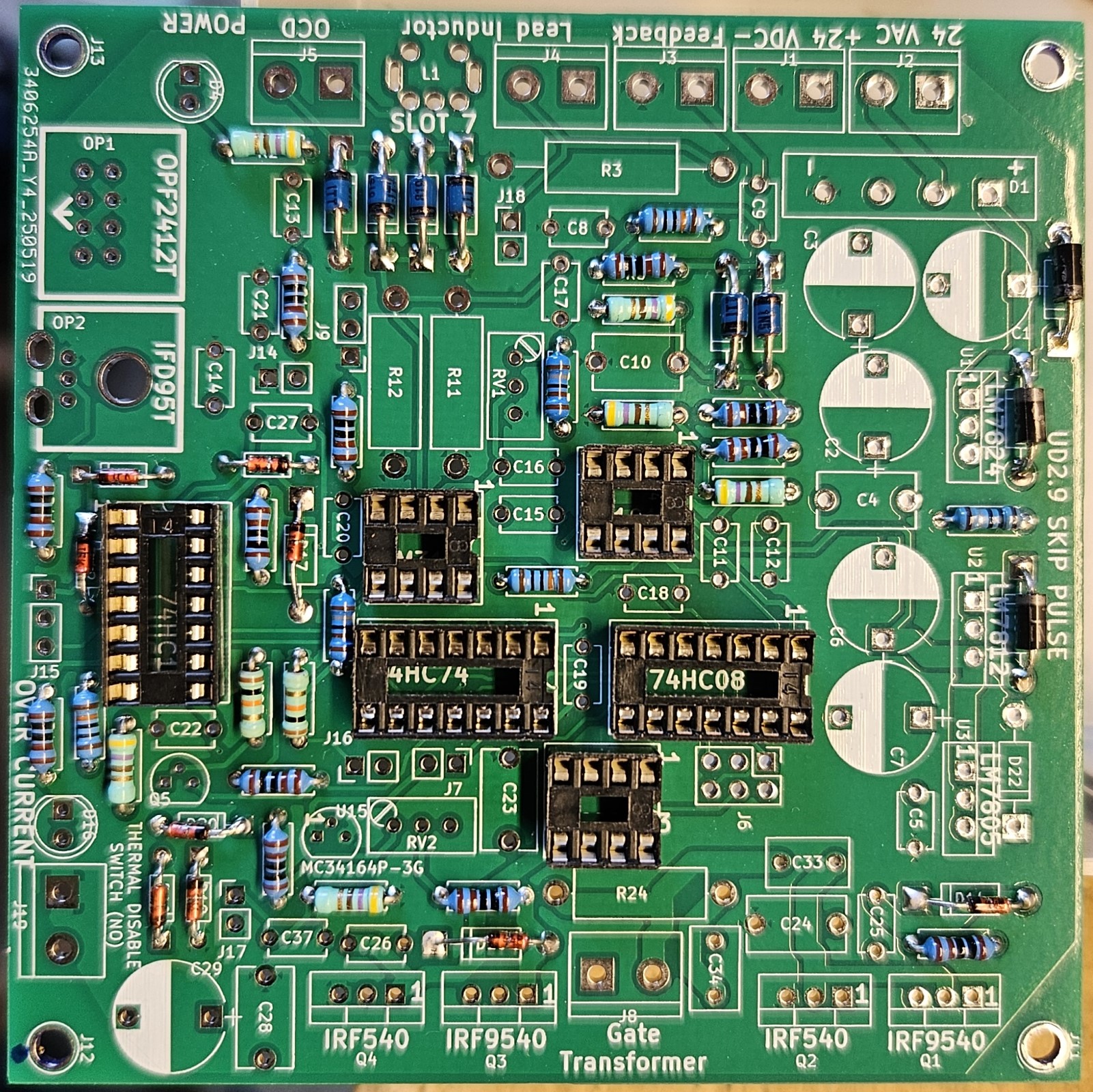
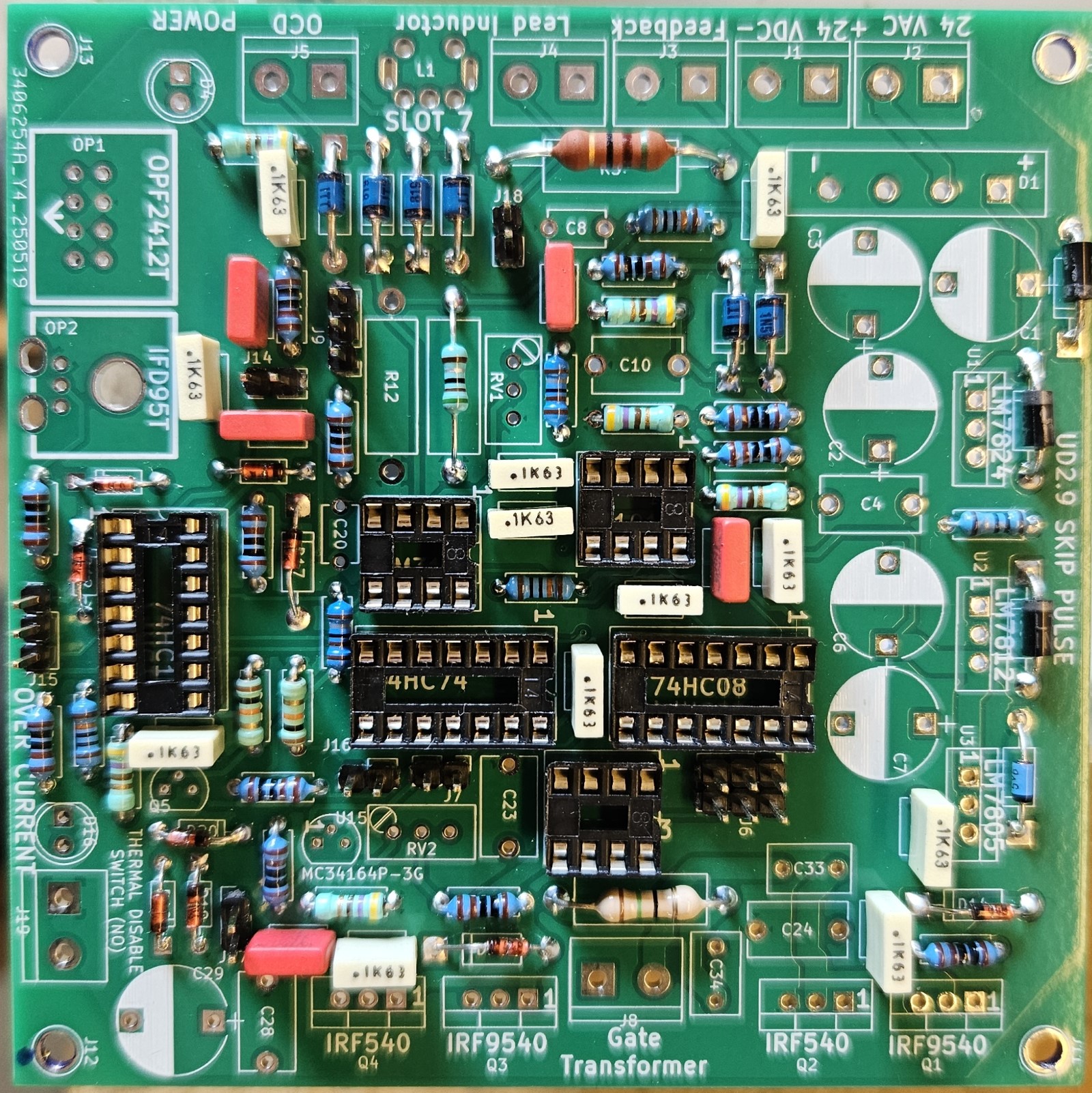
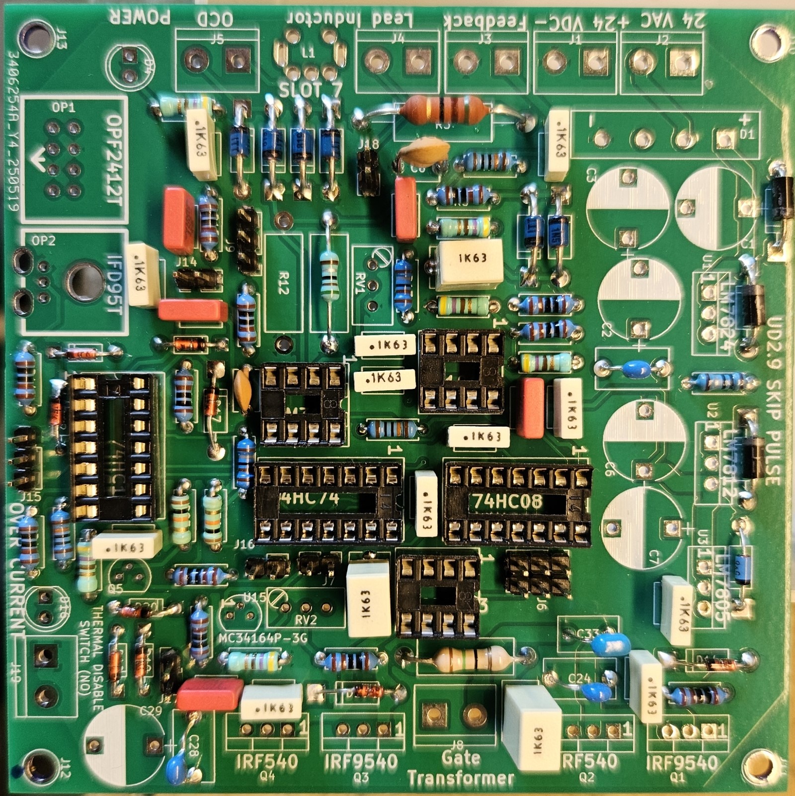
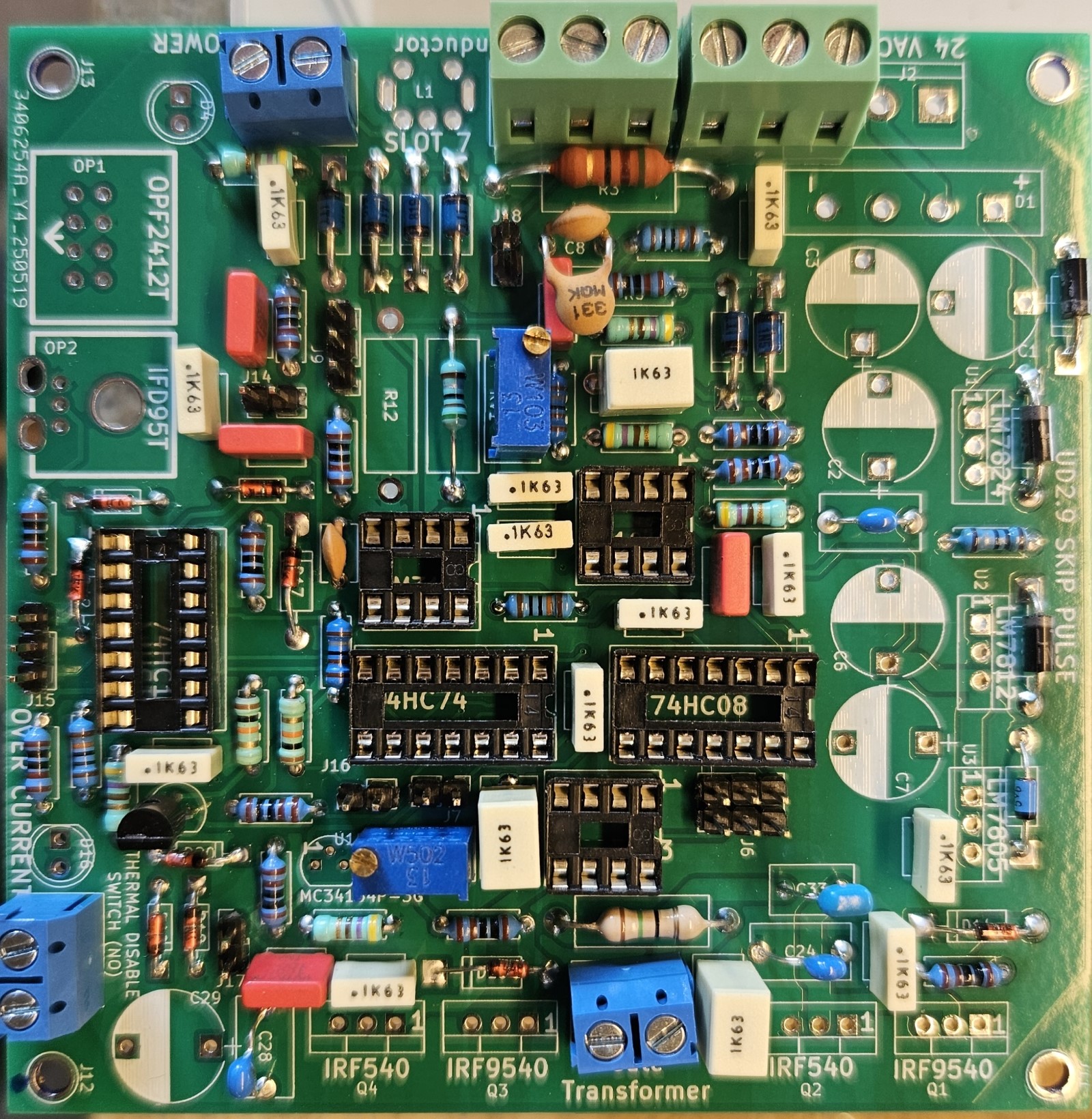
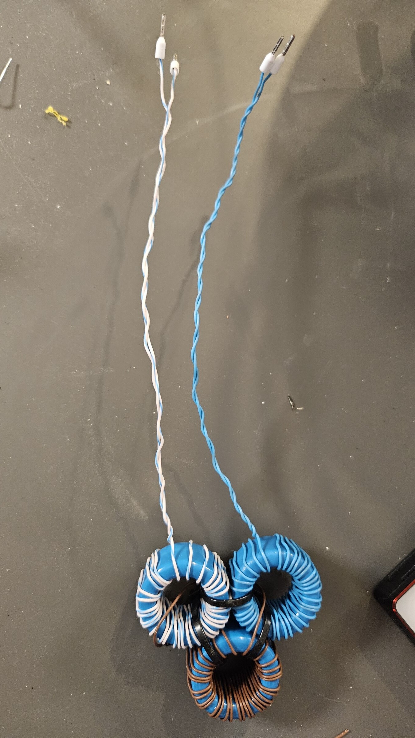
Current transformers was optimized to consume one ring core less. The primary ring core of the cascaded current transformer, has its wire go through two secondary ring cores, for two individual outputs. One output for feedback and one for over current detection, these two outputs can not be combined for the UD1.3 up to UD2.9 drivers.
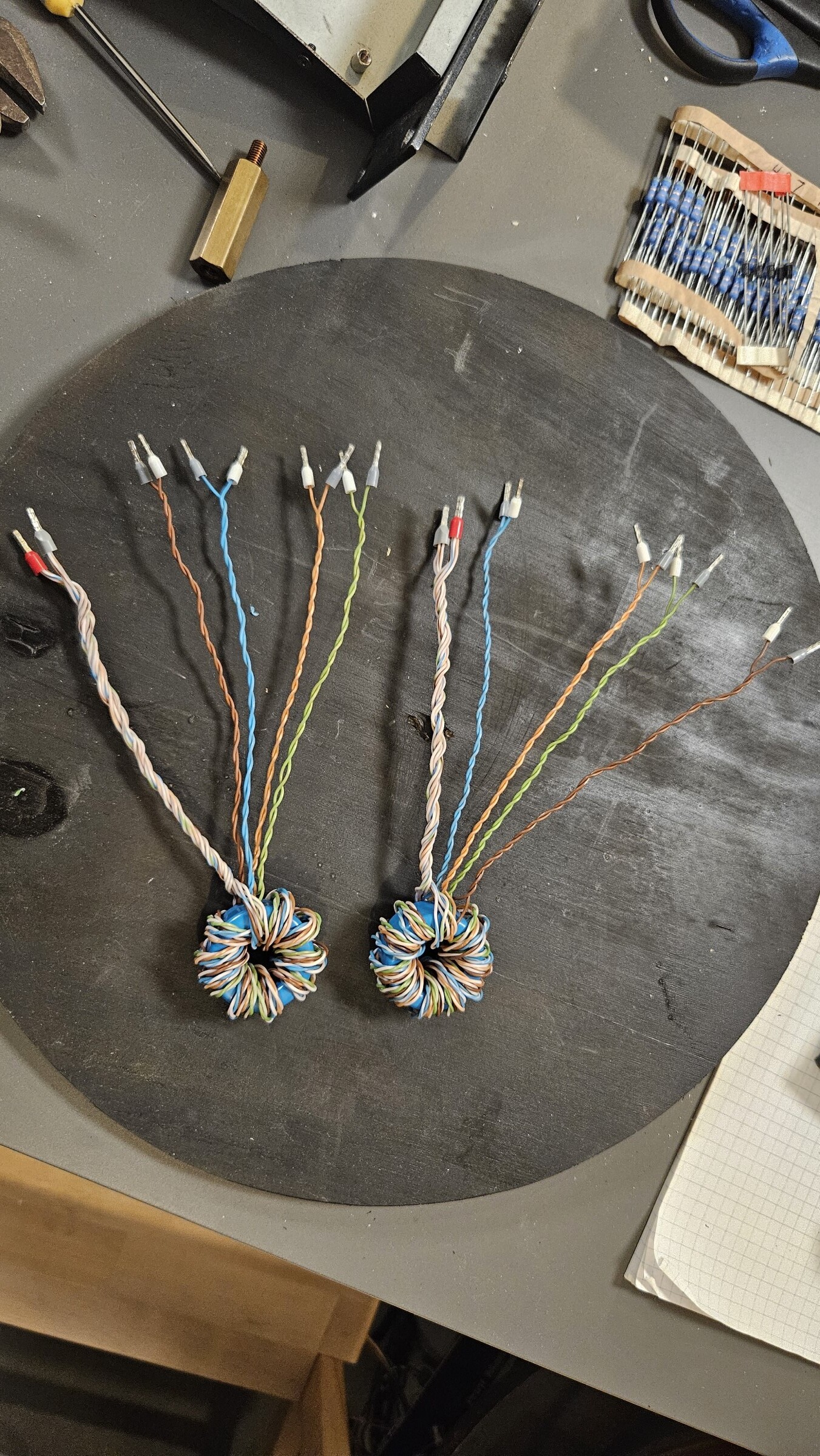
Gate drive transformers was wrongly shown and made as half-bridge transformers. The GDT has to be with 4 outputs for the full-bridge. I was mistaken about pulse skipping drivers needing two individual GDTs, it is free wheeling drivers that needs separate GDTs.
Testing
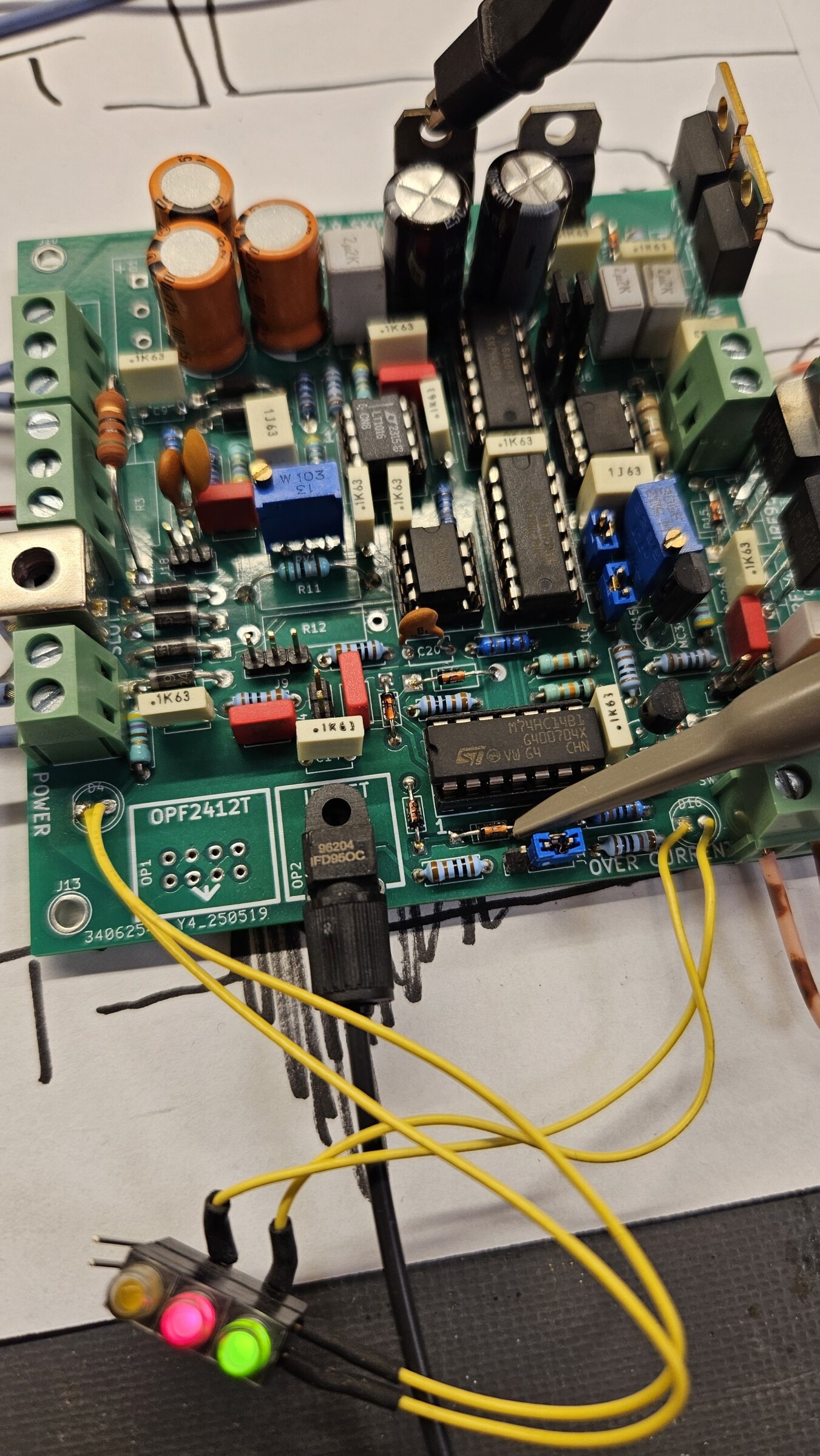
15th May 2026 to 13th June 2026 The testing in this period focusses on configuring and validating the Universal Driver (UD2.9) functions and reforming the DC bus capacitors. Starting up a new electronics circuit can be done with various degrees of precaution. The easy way would be to apply full voltage and all inputs / outputs connected and see that the circuit behaves as designed (or burn to the ground). A more careful approach would be to check power supplies, check single functions and add layers of complexity one at a time.
There is 4 steps that we will go through in testing the UD2.9, but these principles really applies to almost all versions of Tesla coil universal drivers, just omit the tests where those sub-circuits are not present in your driver:
- Supply voltage tests at all voltage regulators, ICs, functions and transistors. Before inserting ICs.
- Interrupter phasing test and adjustment to correct phasing.
- Check feedback input and lockout input to the two AND gates that connects to MOSFET driver IC inputs ENA and ENB. Feedback signal should be a square wave signal at same frequency as the sine wave input on your FB CT connection.
- Check GDT phasing of the outputs connected to the full-bridge of IGBTs.

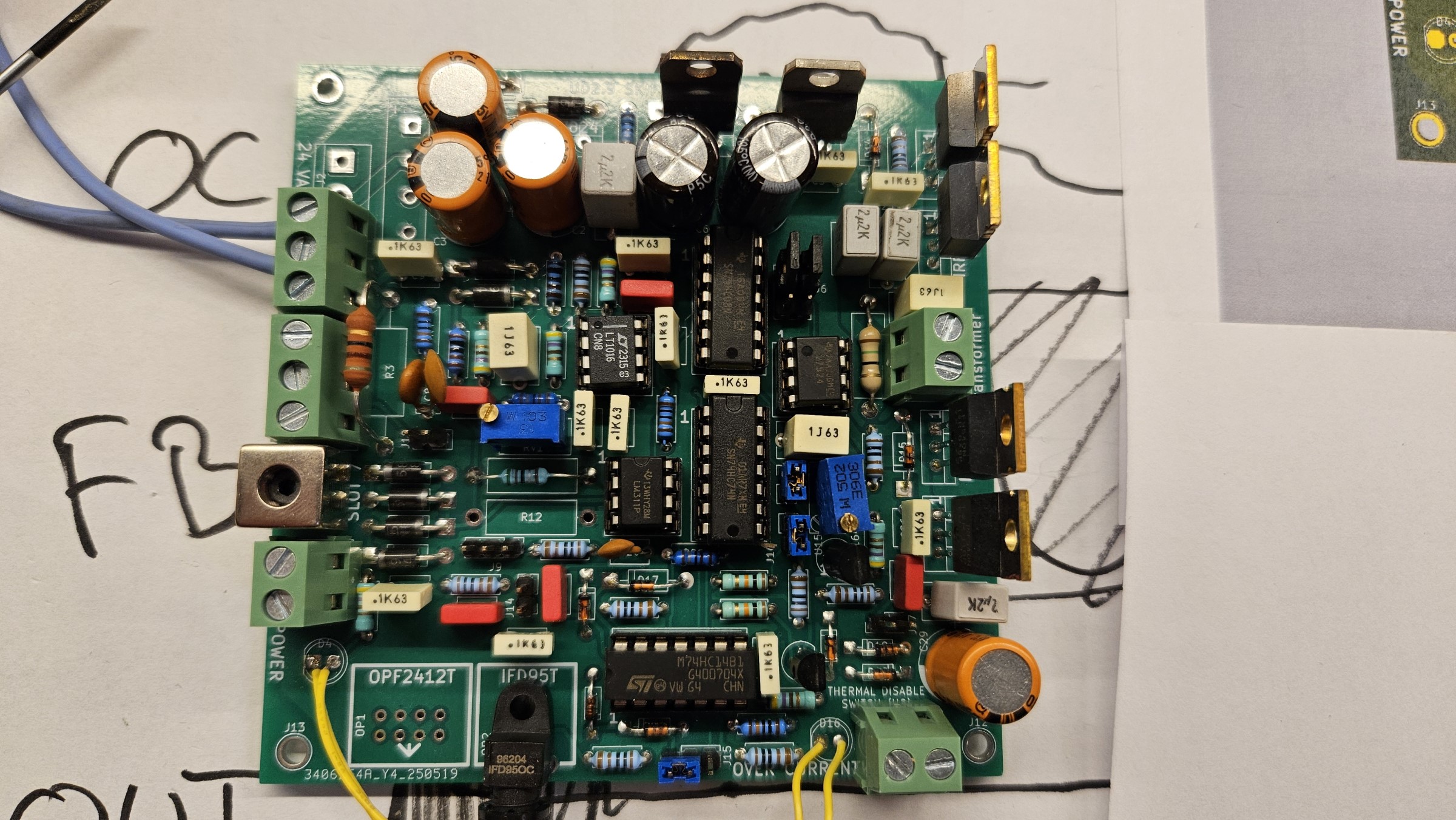
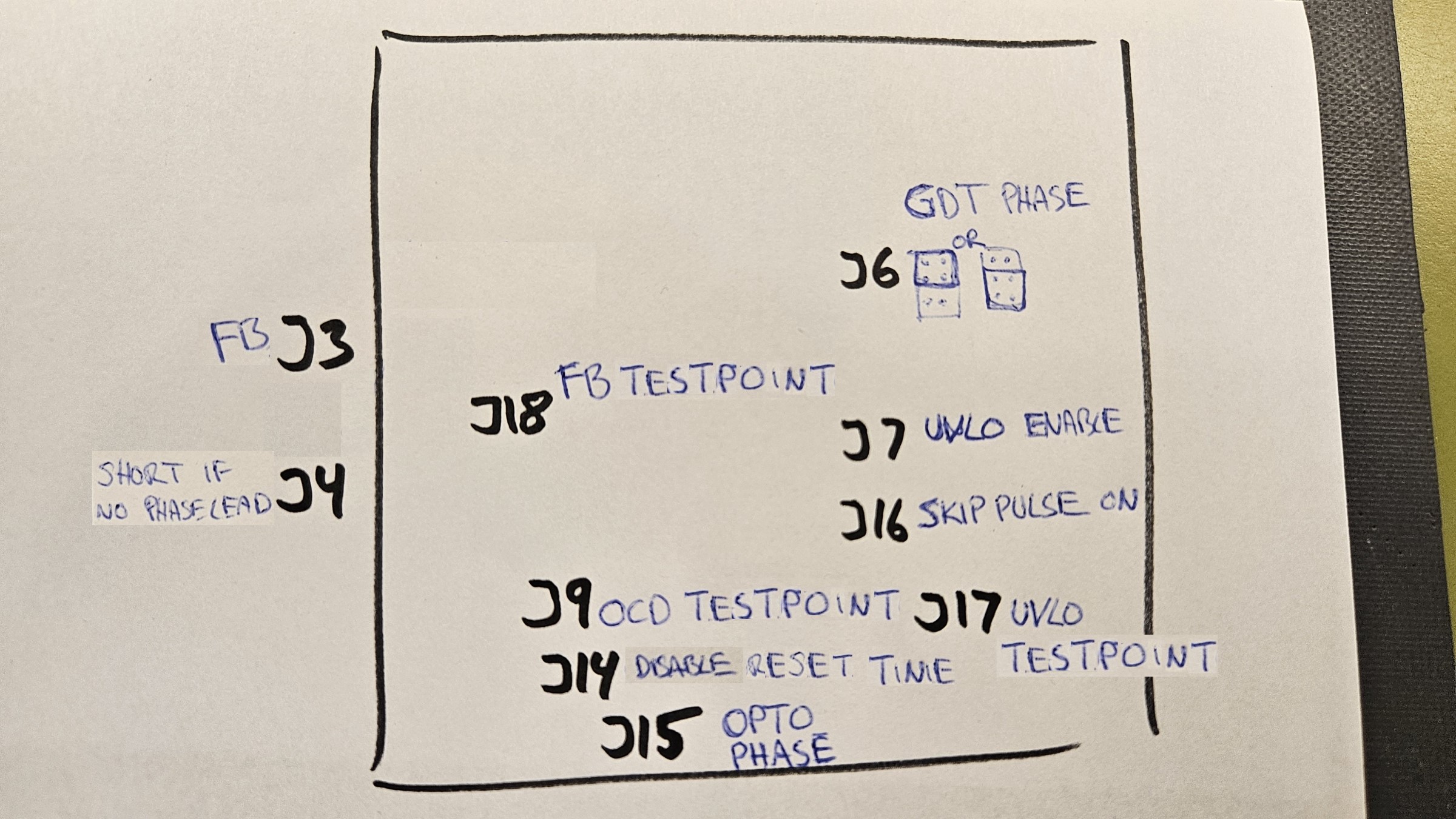
Typical jumper configuration:
- J6 Insert two jumpers top or bottom, they have to be moved in pair, to change polarity of GDT output stage.
- J7 UVLO Enable is for under voltage lockout feature with jumper in.
- J16 with jumper in is for additional flip-flop running a skip-pulse driving feature. Skip-pulse resets the driver faster than waiting for next interrupter pulse.
- J17 UVLO test measurement point. No jumpers.
- J9 is a OCD comparator test point. No jumpers.
- J14 with jumper disables reset time delay of flip-flop. No jumper for DRSSTC.
- J15 with jumper in left or right side, chooses polarity of optical interrupter input.
- J18 is FB CT measurement point. No jumpers.
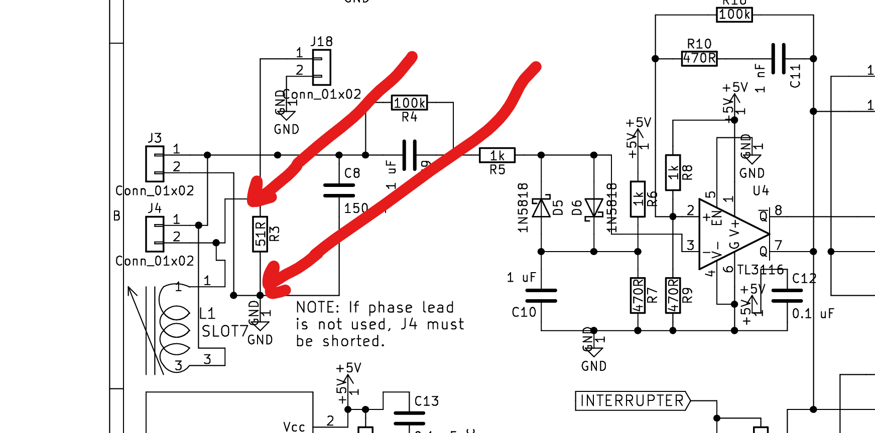
- J4 terminal is to be shorted if no phase lead inductor is used. Feedback CT always goes to J3.
Capacitor reforming is necessary when a electrolytic capacitor is left unused for extended periods of time, years after years and to start with are used capacitors, reforming is recommended. There is a risk that the electrolyte is not completely covering the plates, that it being cold is taking up less space or oxidization layers have formed.
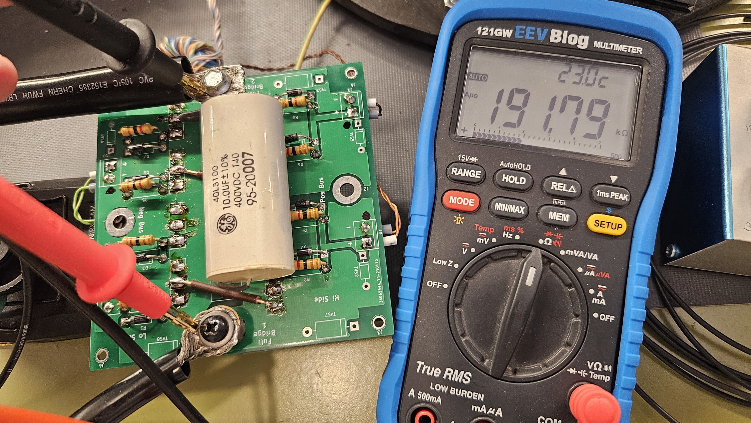
There is a general recommendation, that reforming has to be done over the same amount of hours, as the same amount of years, the component have been in storage. That translates from 5 years on the shelf, to 5 hours of reforming. There is two “methods”, either slowly increasing the voltage or stepping up voltage. We also need two multimeters to watch both the DC voltage across the capacitors and a multimeter capable of showing current in milliamps, to watch the charging current.
- Use a variac / variable transformer / auto-transformer with a full-bridge rectifier for slowly increasing the voltage during the process.
- Use steps of 100 VDC input voltage, with a current limiting resistor keeping current at a maximum of 100 mA.
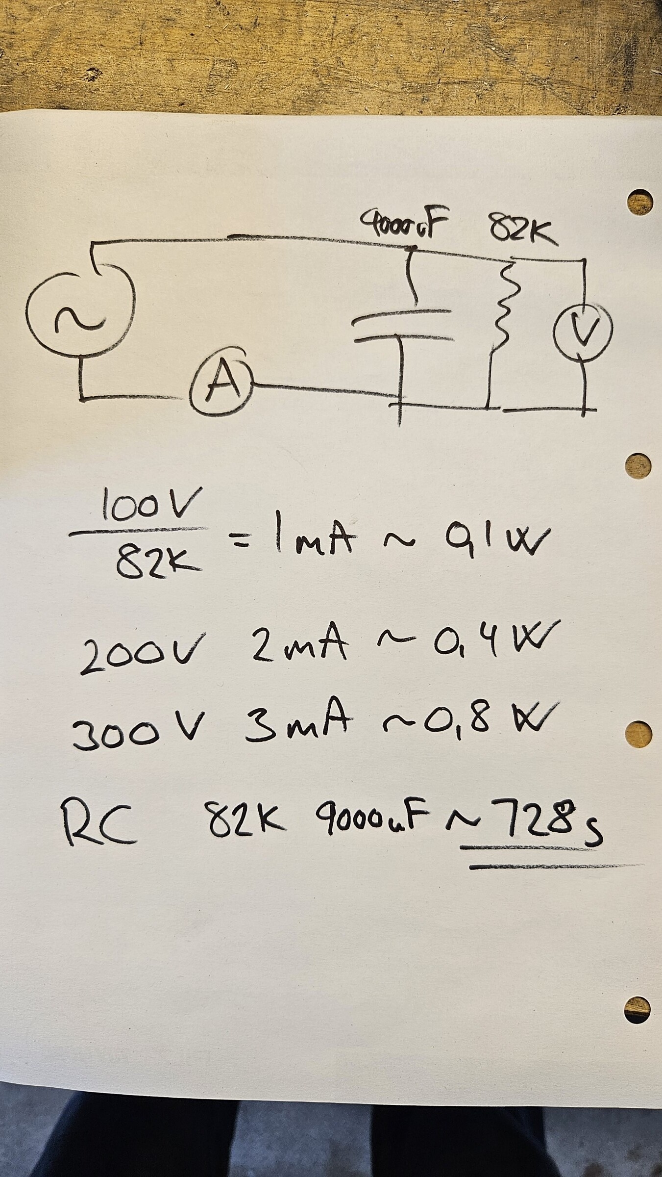
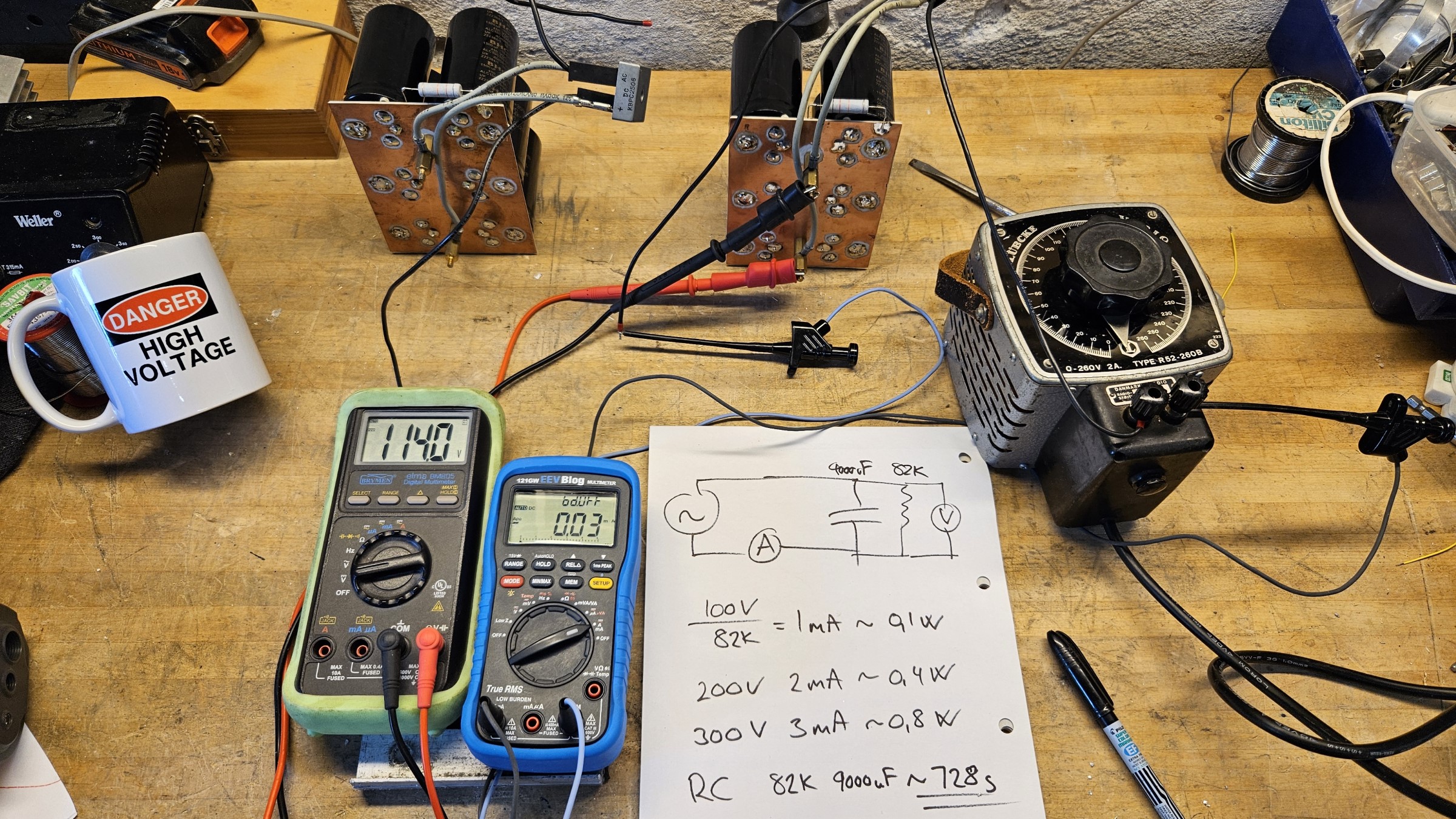
An empty capacitor looks like a direct short-circuit to a power supply. This high inrush current can destroy an old and cold capacitor. Ensure your capacitors are at room temperature before this process begins. A cold capacitor subjected to a large inrush current is very likely to fail with a internal flashover from the sudden stress.
Expected capacitor life time in Tesla coils is normally not of great concern. 95% of all Tesla coils will most likely NEVER run for more than 10 hours. So we do not need perfectly reformed capacitors or we can even abuse them a bit from not properly overhead in ripple current capability.
Capacitor datasheets will normally state the allowed leakage current for a capacitor to be healthy. Once a voltage level is reached, we leave the capacitor at this level for a little while and see that no current is flowing.
Practical tests, Softstart, Secondary Coil Terminations and Explosions
14th June 2026 to 3rd August 2026 In this part it is all about practical testing and that includes full mains power startup, secondary coil terminations and connections, adding a new soft start module to the mains input for dealing with high inrush current and blowing the full bridge of IGBTs up completely.
The issues I encountered during this part of the building and testing is also being discussed at High Voltage Forum: https://highvoltageforum.net/index.php?topic=3623.msg26734#msg26734. This is setting me back to either try to fix the full bridge PCB or build new full bridge PCBs for TO247 devices or just move on to IGBT bricks instead.
I should have:
– Tested my IGBTs before soldering the bridge PCB
– Tested more with just driver and bridge, no high voltage
– Used a variac for low voltage testing of the complete system
The coil powered up fine, driver in shutdown state until interrupter signal comes.
Then nothing happens, no oscillation, so here is things I tried:
– Change polarity on GDT jumpers on the driver
– Change polarity on feedback CT by switching leads around in terminal
– Reduce CT ratio from 1:1000 to 1:200
I then decided to try startup oscillation with a signal generator set at resonant frequency (270 kHz) and inject that shortly by hand to see if that could get it running. But I got punished instead. DC bus at 320 VDC and interrupter set at 120 BPS and very low on-time (I hoped that was enough to save me in failure cases)
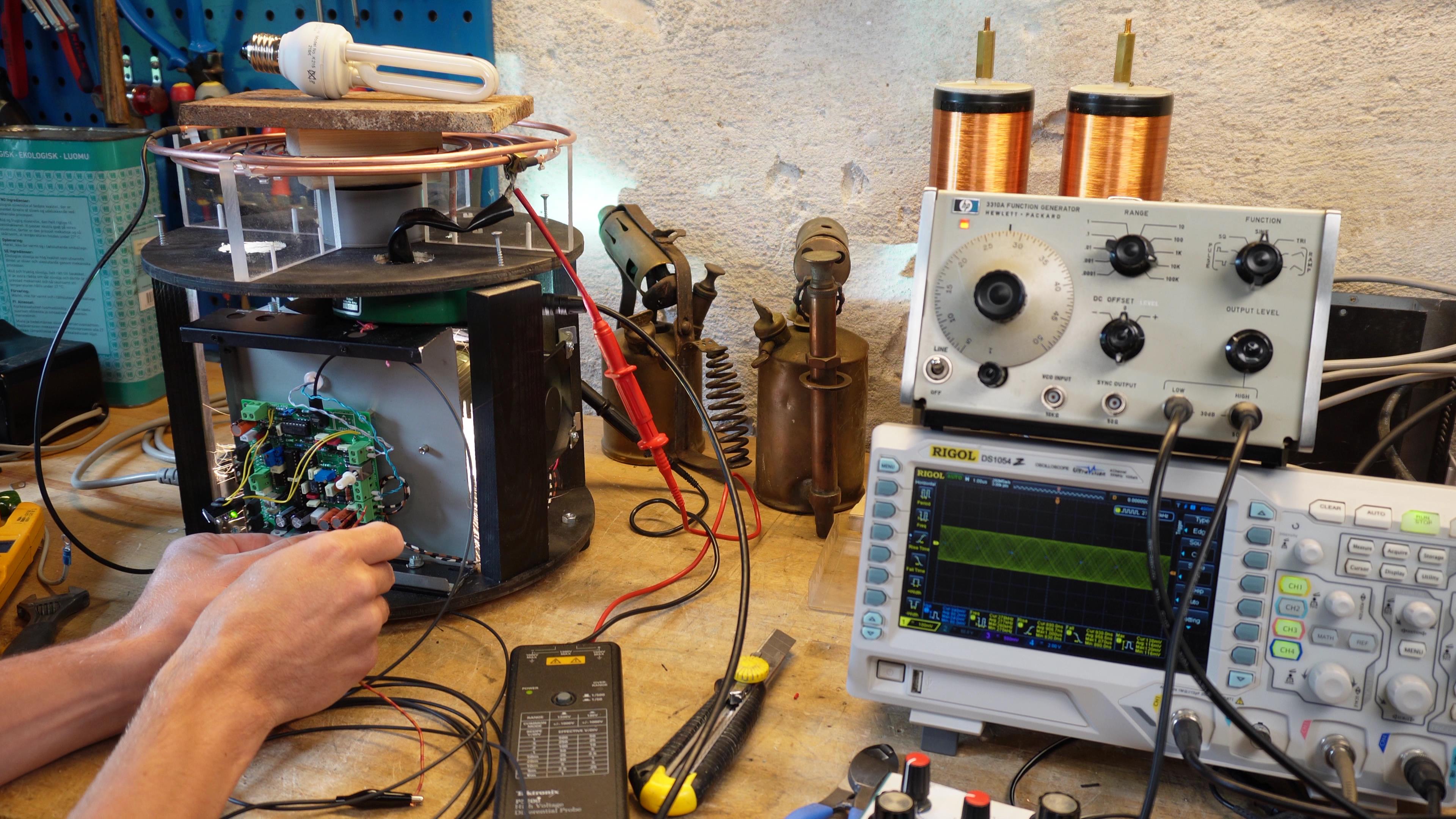
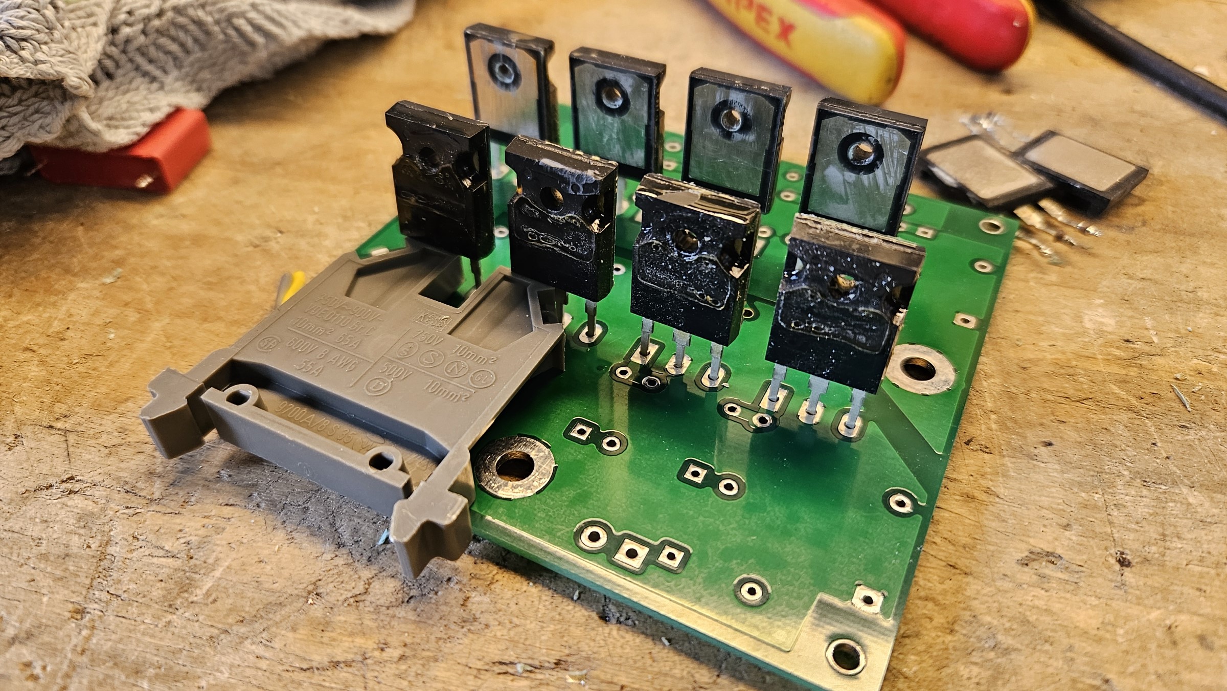
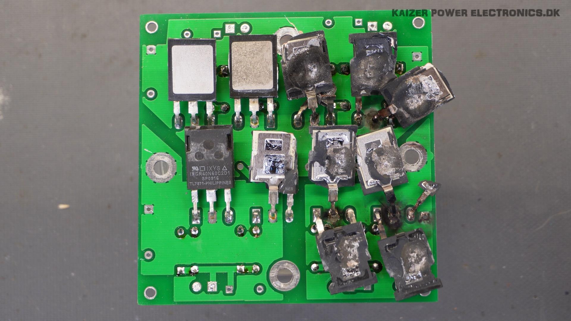
Inspecting the burned PCB shows that Q5,6,7 and 8 is now with black scorch marks, funnily enough the IGBTs seems fine, its the traces of the PCB that has been blown out. It seems that all collectors melted the tracks away. The pads also only have these 4 small bridges to the plane, not full connections (for easier soldering).
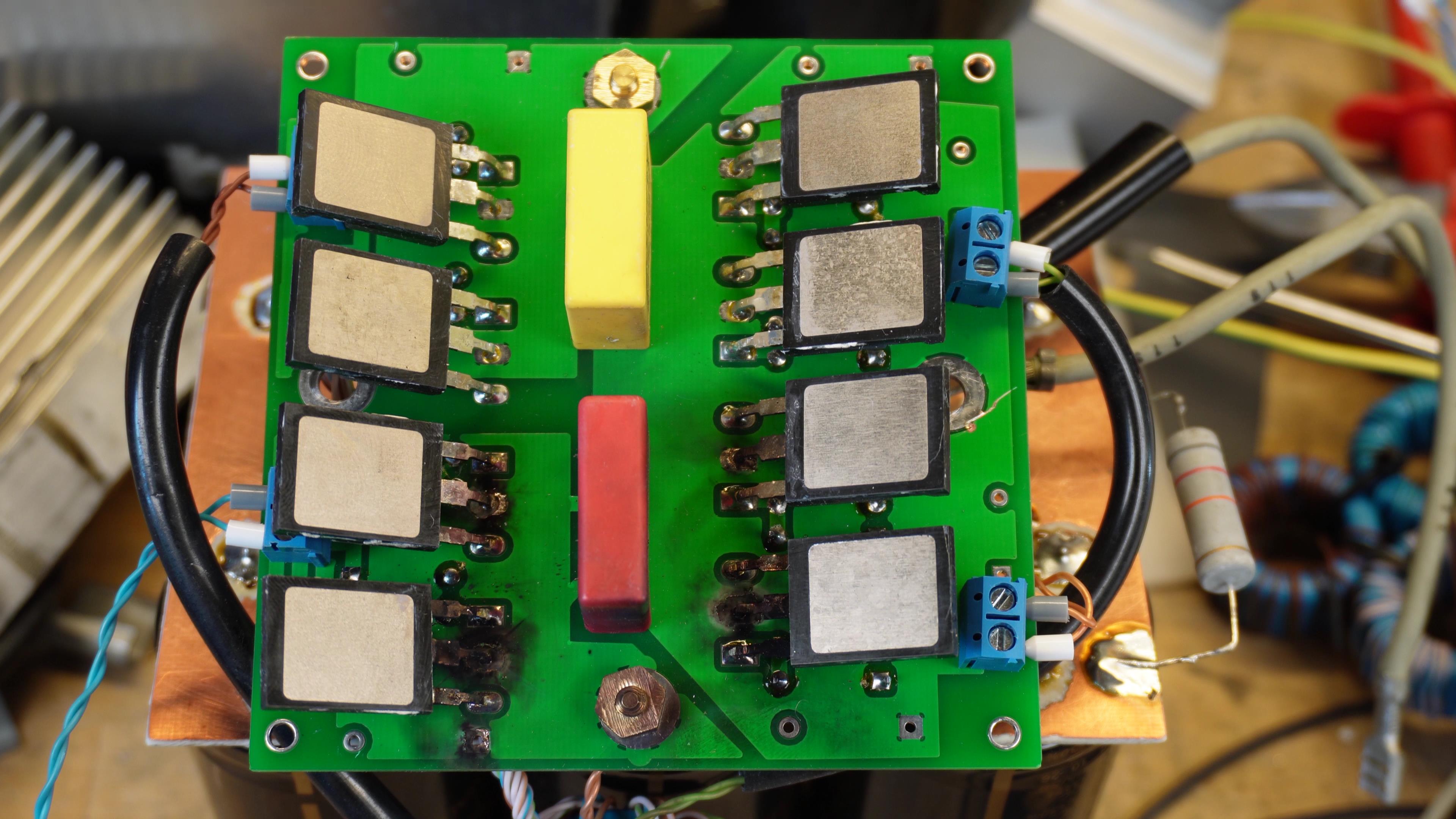
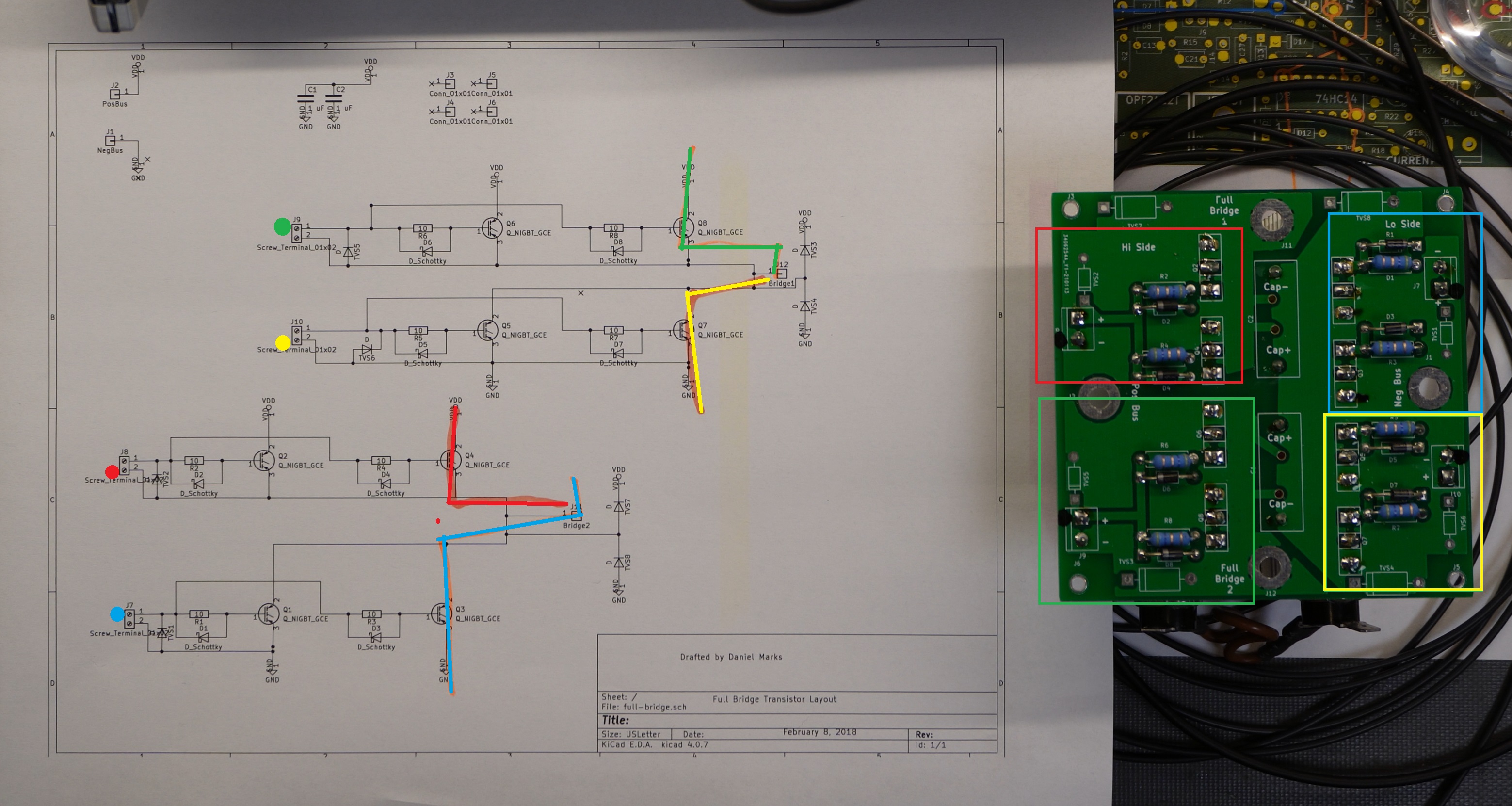
I double checked wiring, GDT winding, schematics and bridge PCBs to look for errors that could result in this total short circuit from what seems like wrong phase of driving.
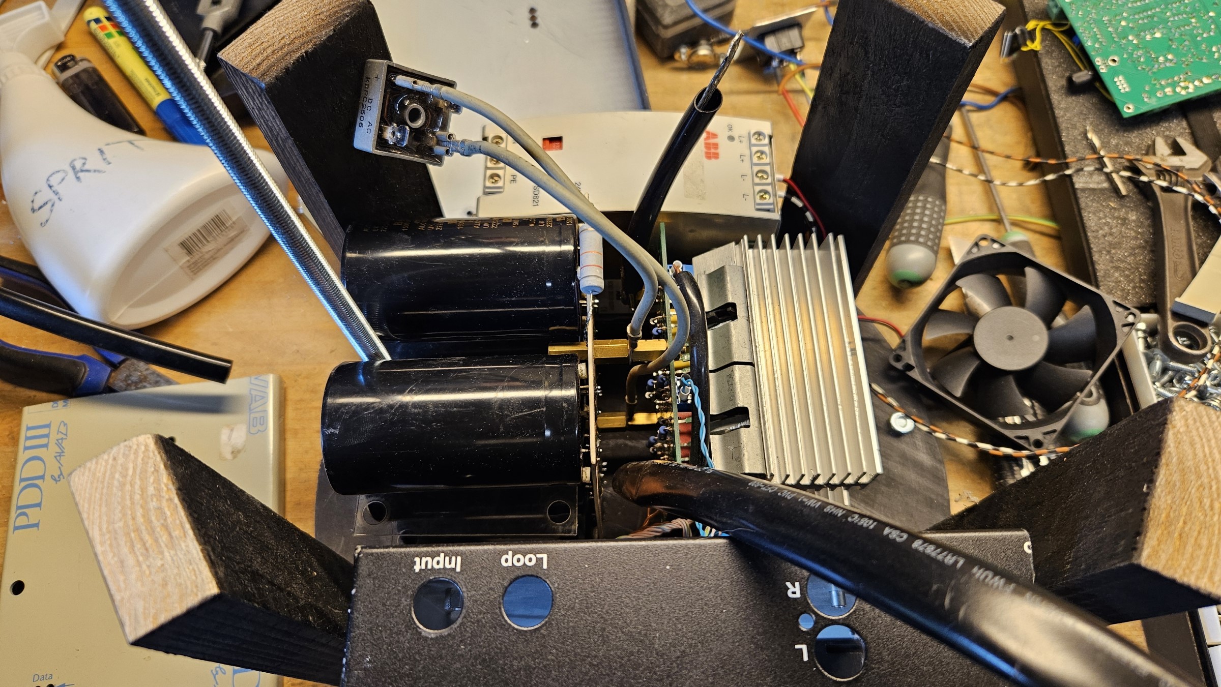
I initially thought the Tesla coil base, with its 30 cm diameter, was going to make plenty of room for components. It quickly turned out to be very crammed and near impossible to add more needed components. Sensitive components is protected with layers of plastic, mostly for mechanical protection against wires rubbing up against sharp PCB edges and such.
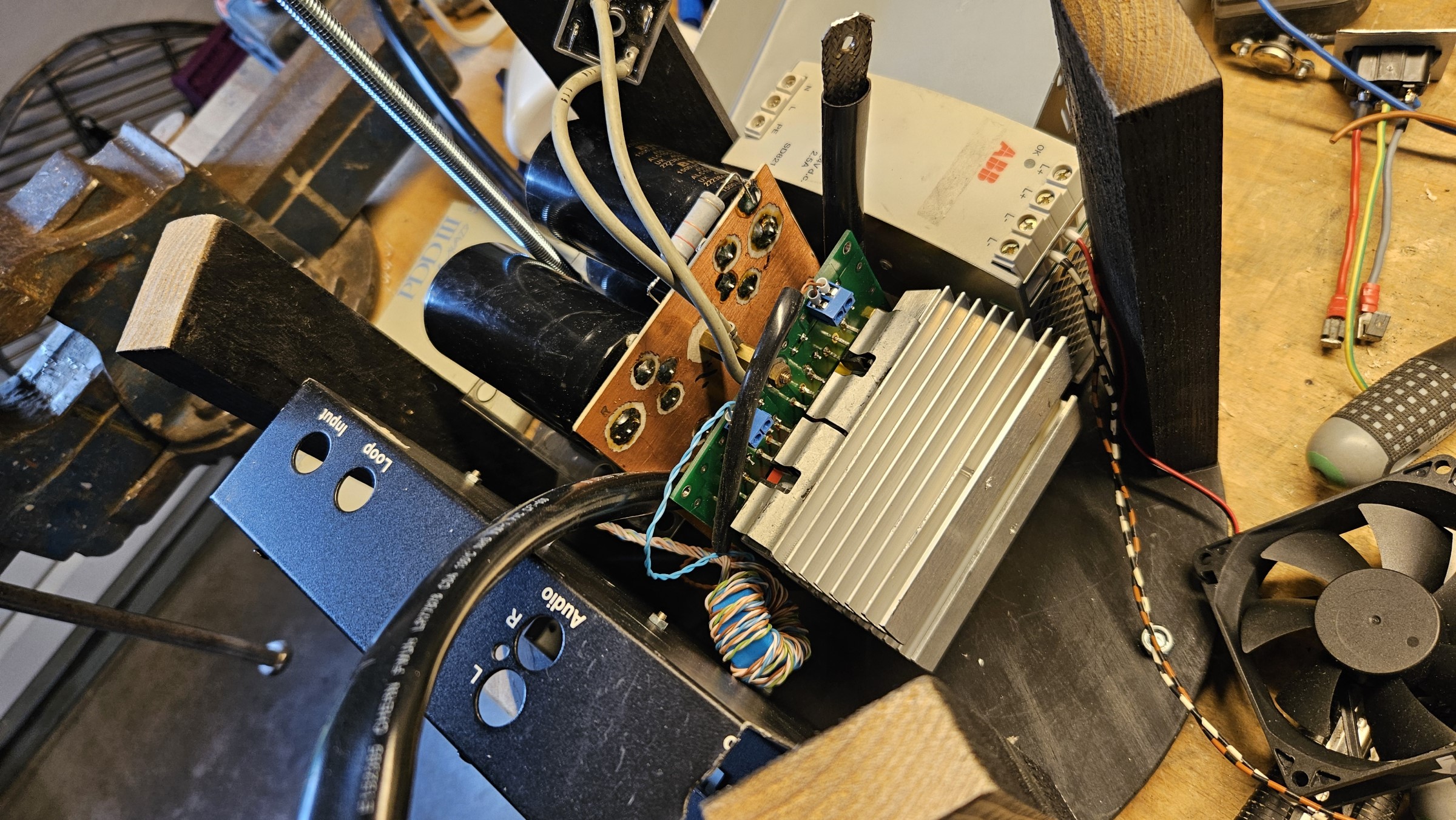
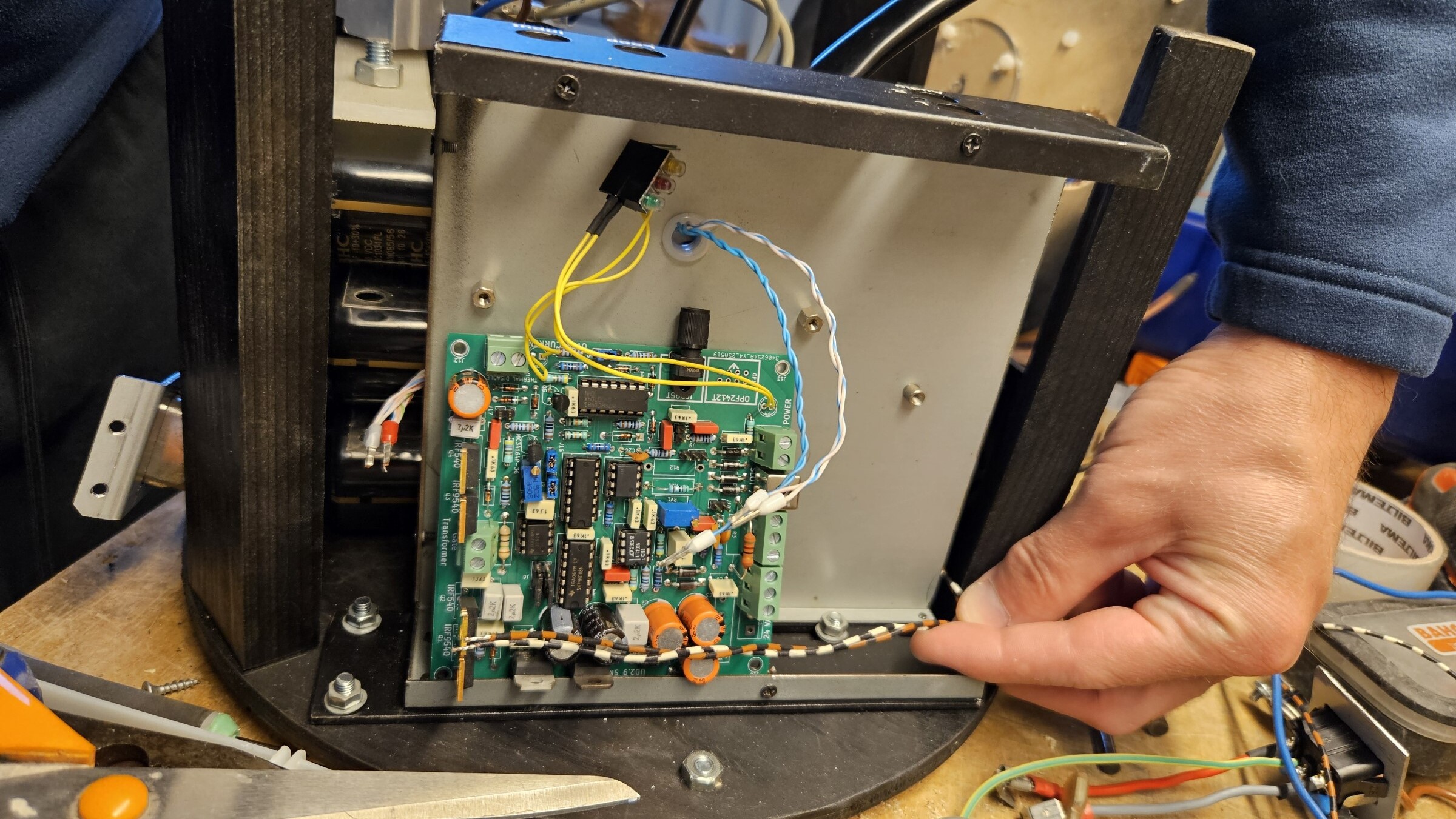
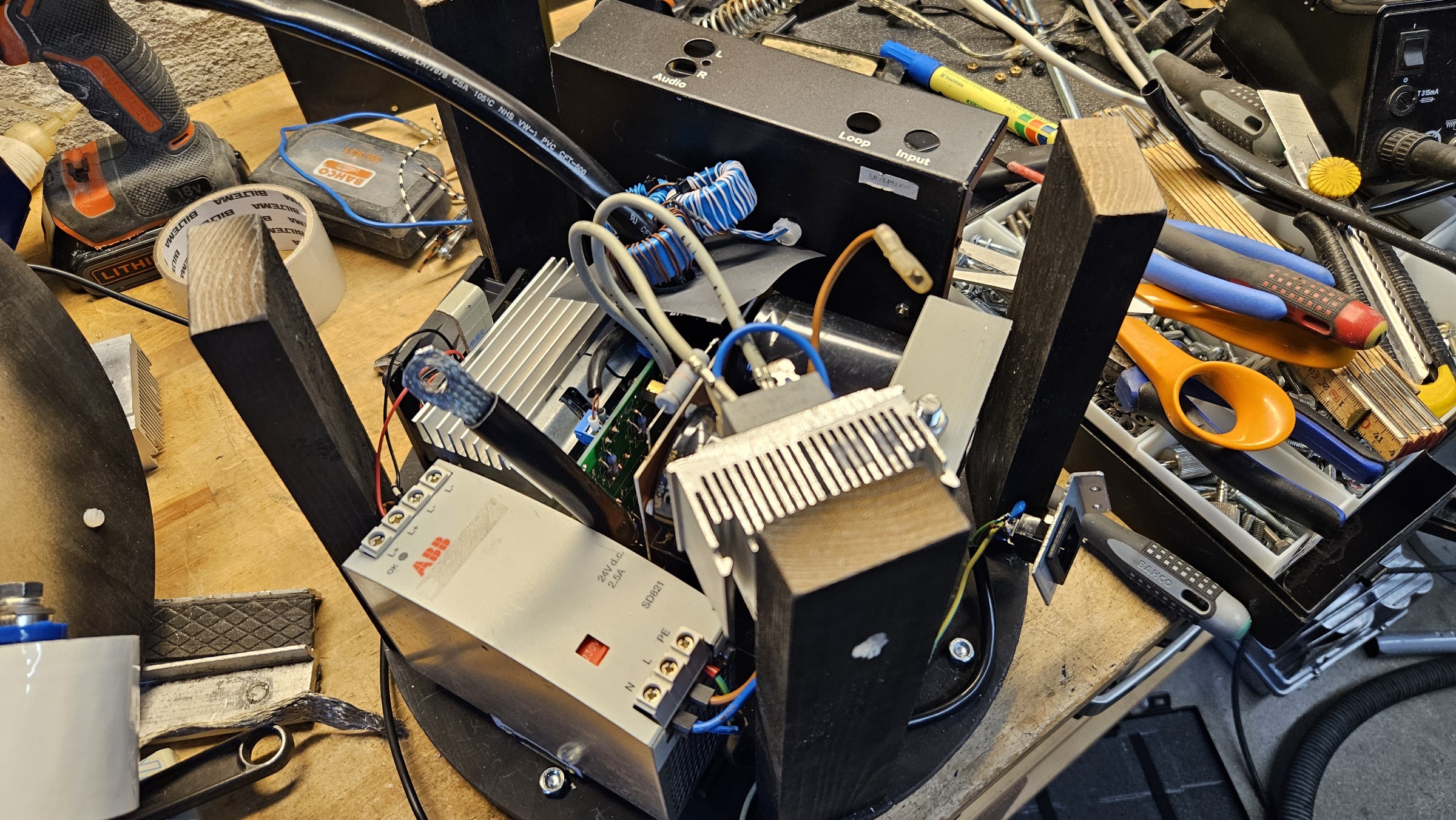
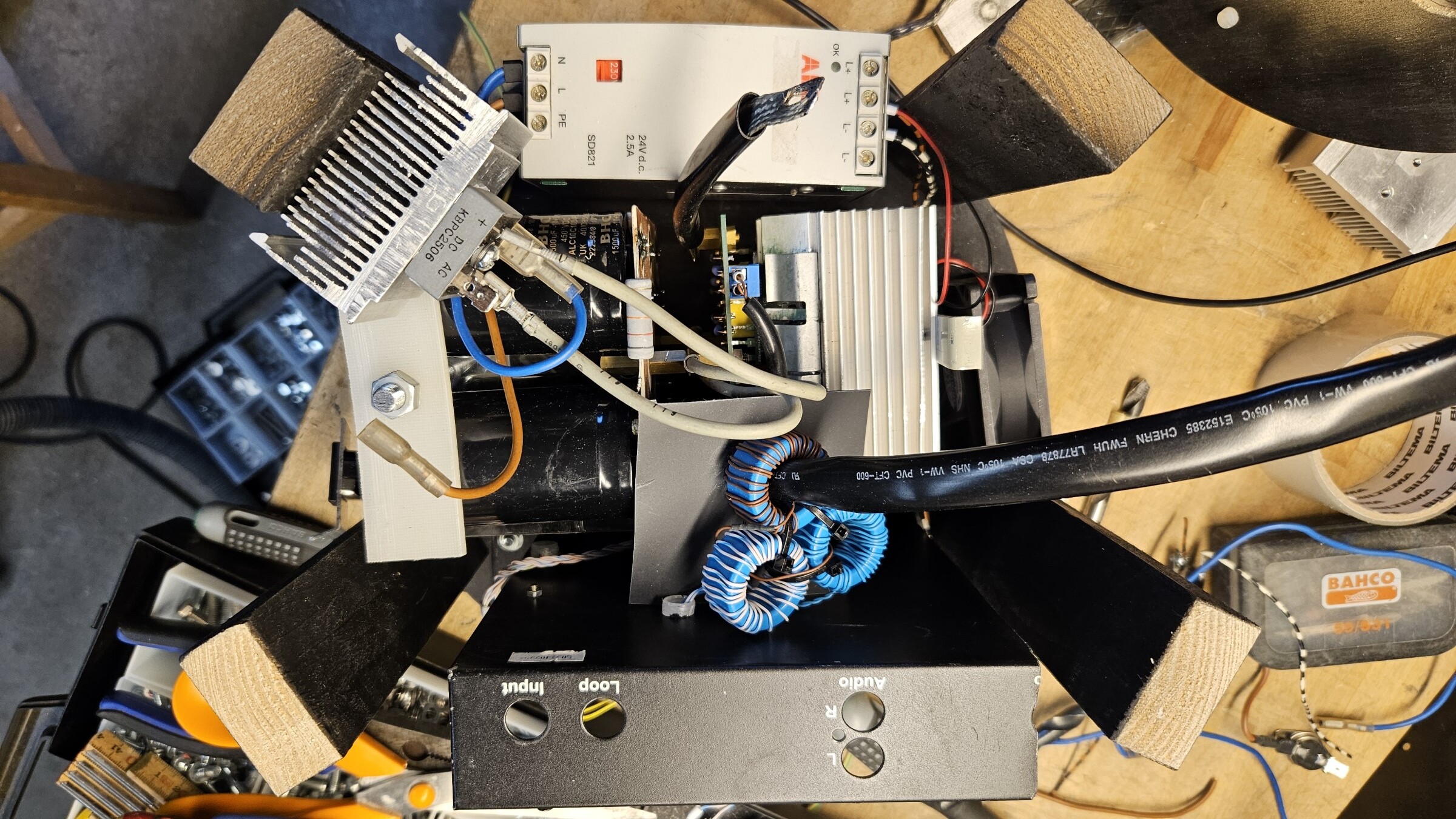
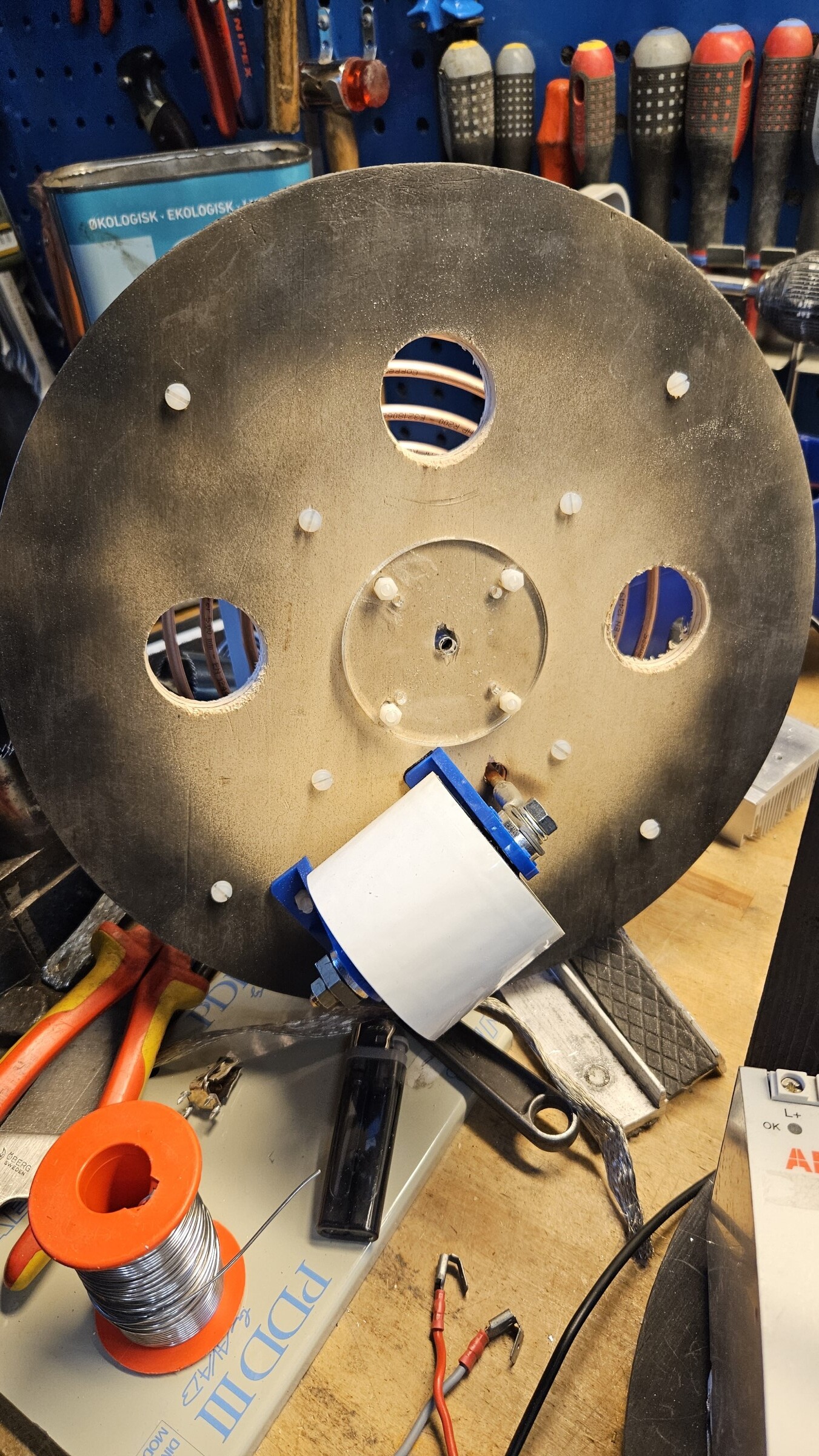
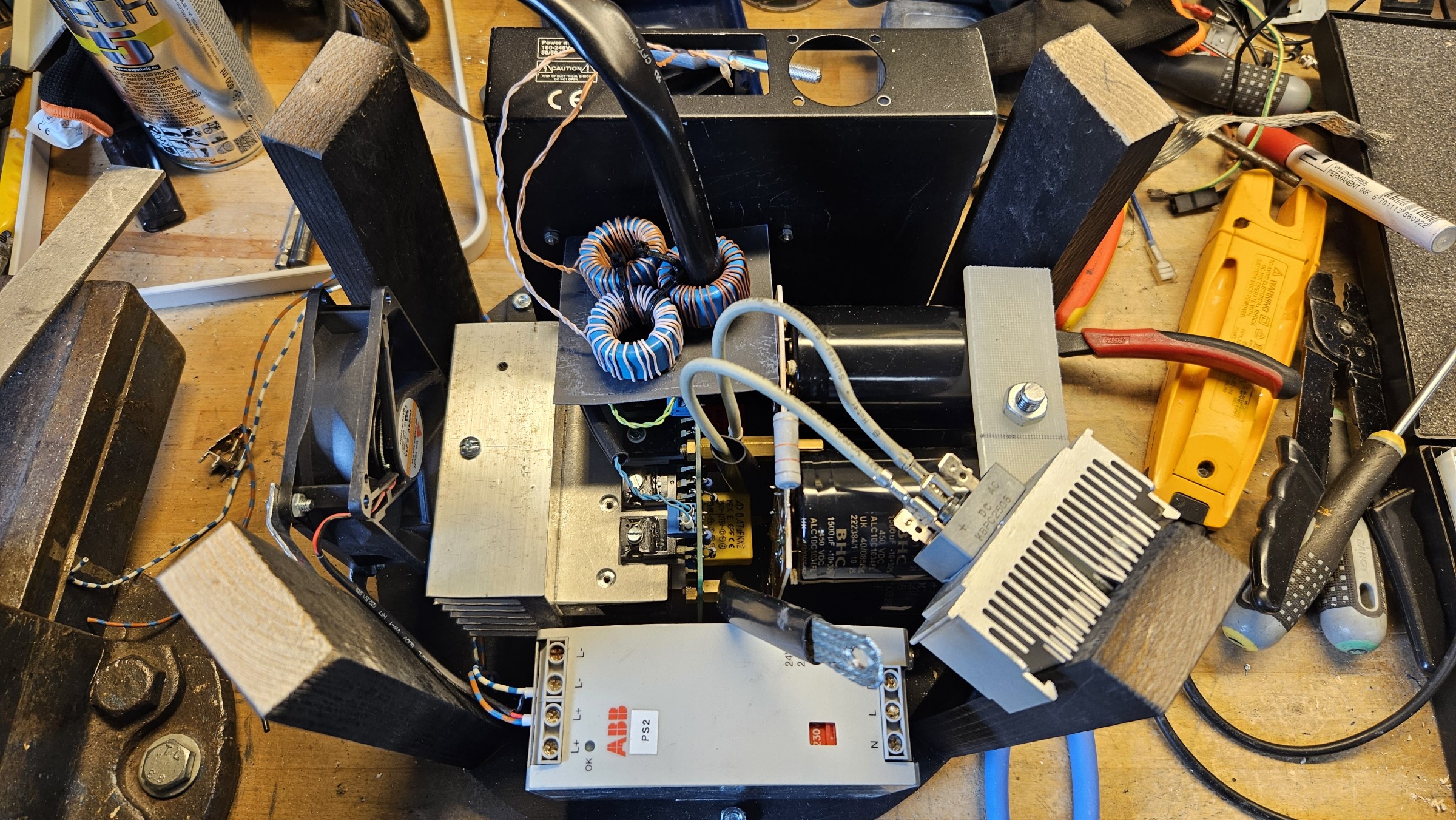
I used a 5 Ohm NTC for soft start circuit and capacitor precharging, but it proved to be extremely too small to handle the inrush current of 9000 uF, at least in the scope of the mini circuit breakers tripping from the still high inrush current through 5 Ohm.
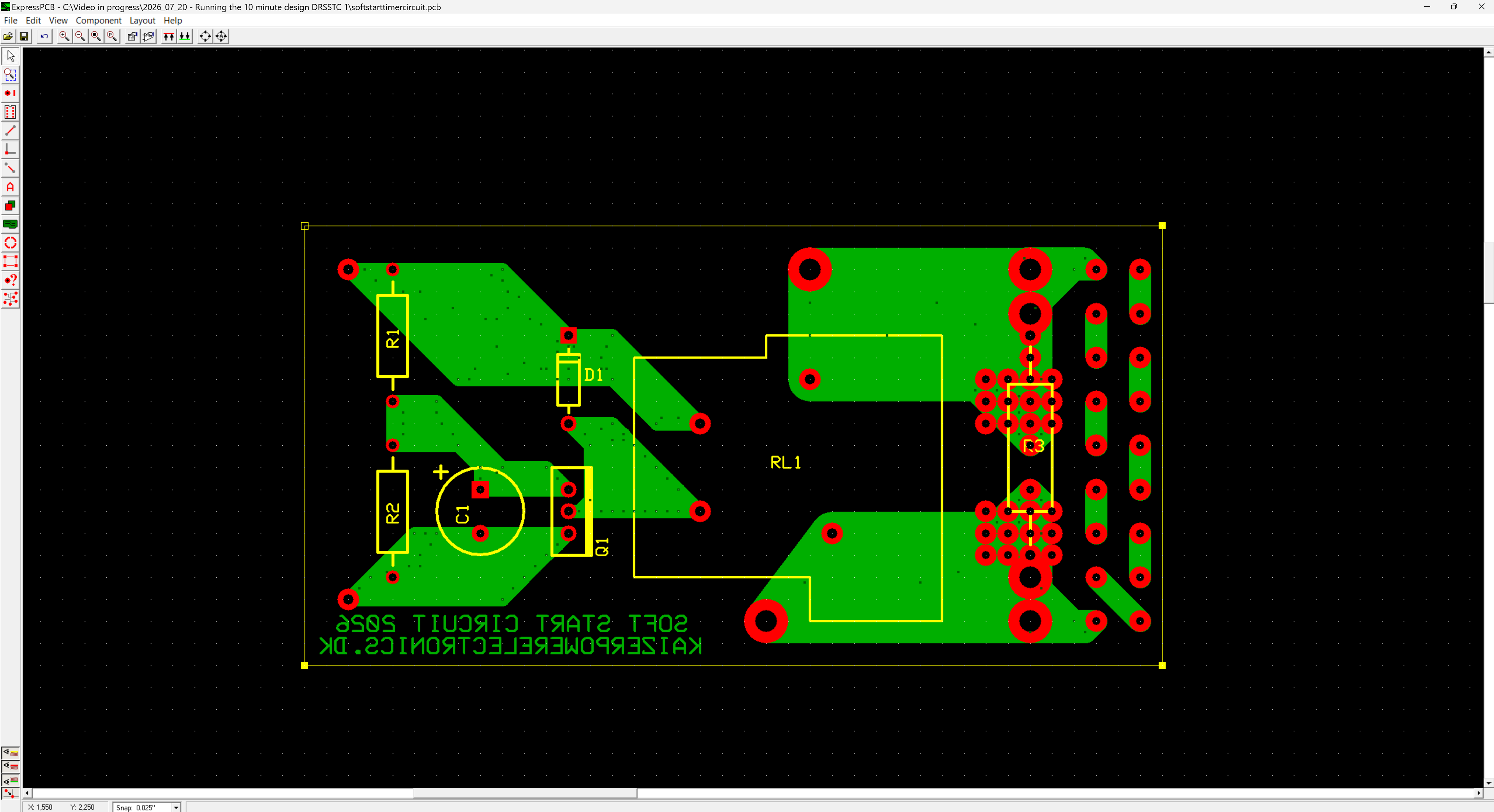
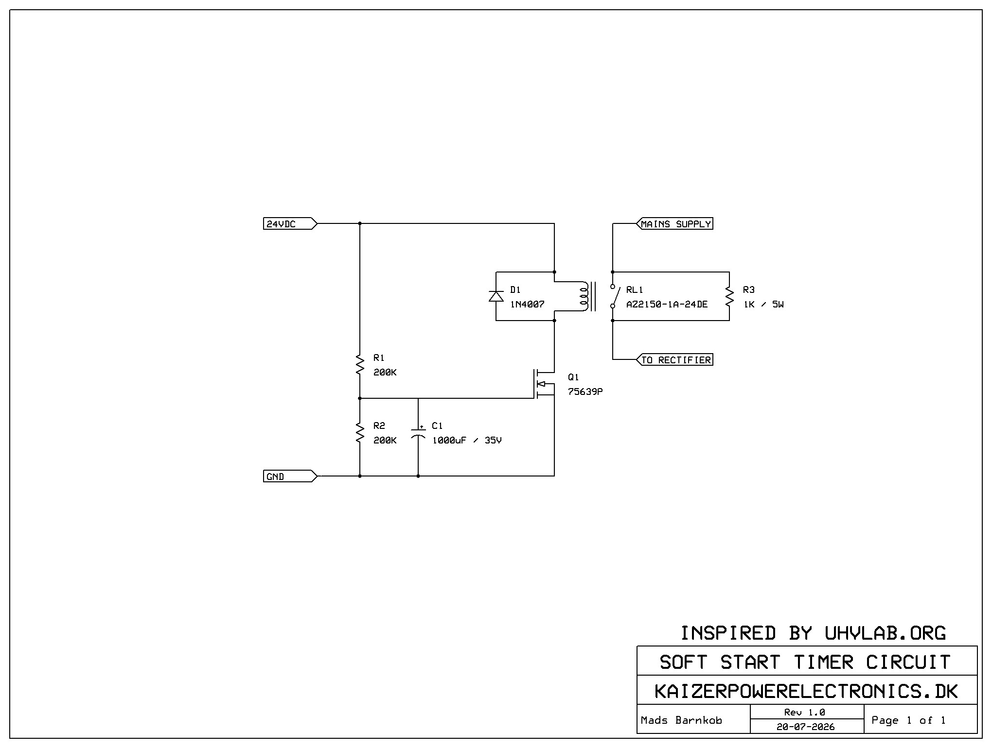
Being forced to use large normal power resistors, a contactor and timer is needed to bypass the resistor after precharge is done. I found a equivalent circuit on UHV Labs and made a version of it to the components I already had. I adjusted the component values to suit my needed precharge time for the 9000 uF electrolytics capacitor bank, so it would not trip my C13 breakers.
Schematics: https://kaizerpowerelectronics.dk/files/projects/2026_02_08_-_kaizer_drsstc_vii/softstarttimercircuit.sch and PCB layout: https://kaizerpowerelectronics.dk/files/projects/2026_02_08_-_kaizer_drsstc_vii/softstarttimercircuit.pcb
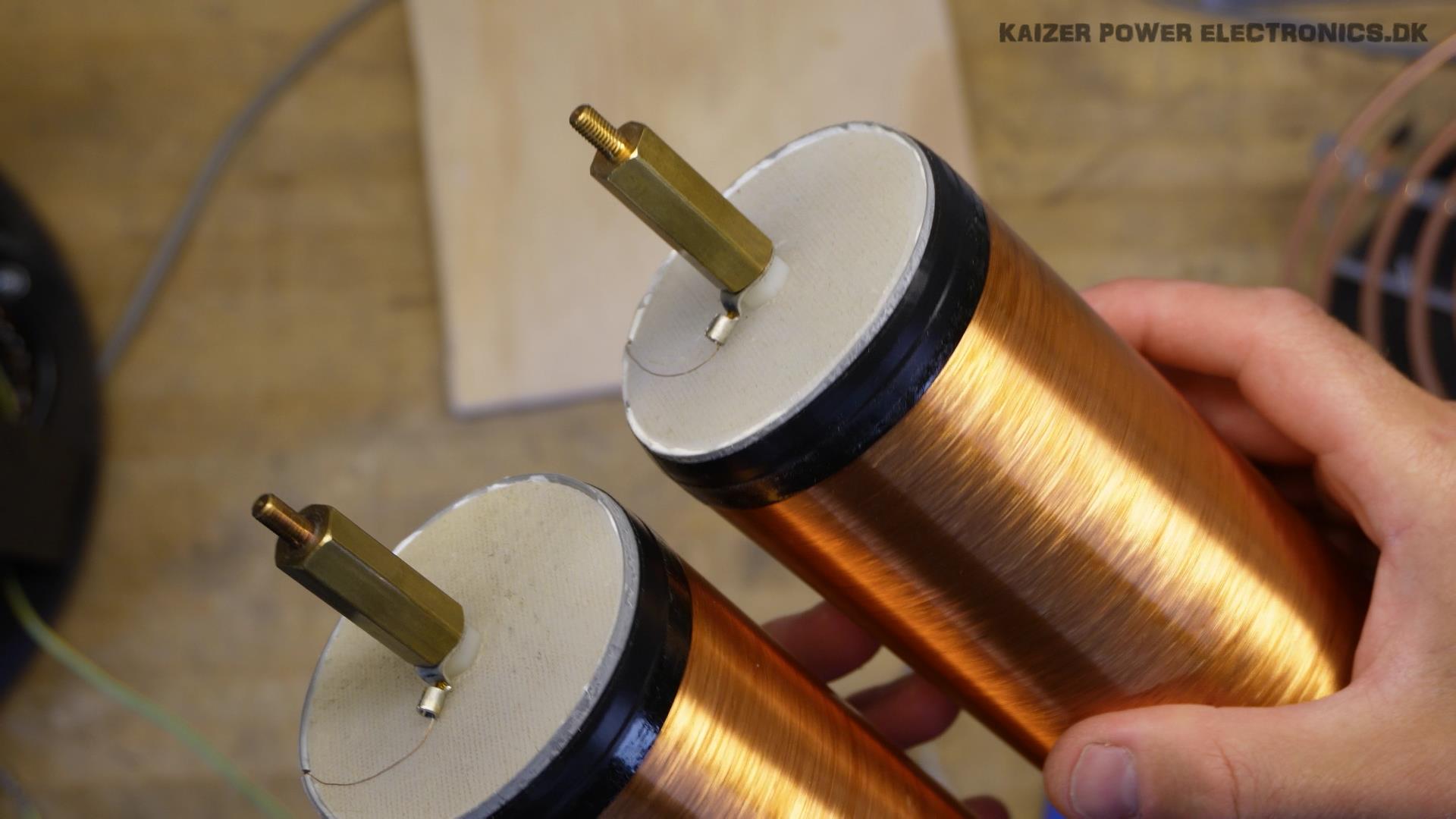
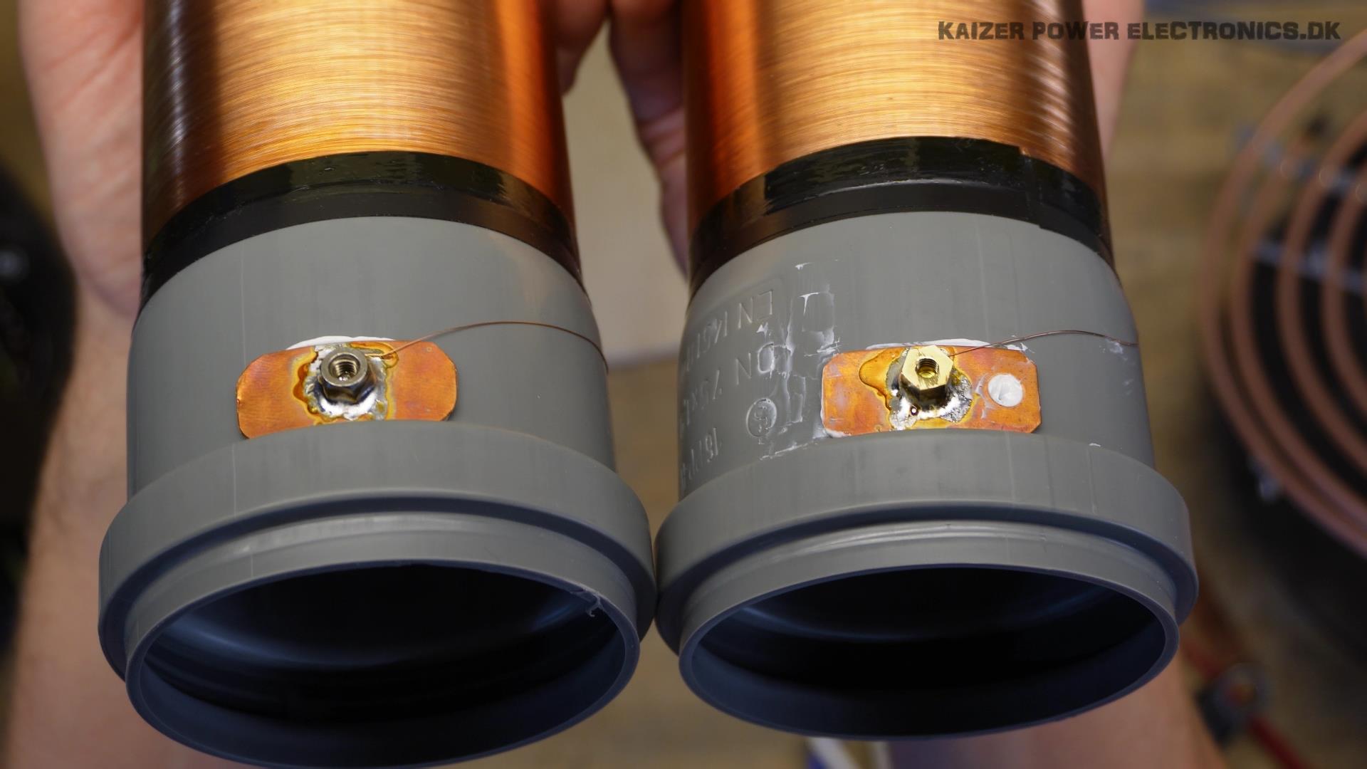
Topload termination is a simple ring cable lug, with plastic removed and secondary coil wire soldered into. Be sure to orientate the wire in a soft curve to not stress it from heat expansion and protect against mechanical stress from topload moving.
RF ground termination is a piece of copper strip with a brass nut soldered onto it. Be sure to orientate the wire in a soft curve to not stress it from heat expansion and protect against mechanical stress from secondary coil or RF ground connection moving.
Rebuilding the Inverters with new TO-247 IGBTs
4th August 2026 to 29th August 2026 Problems with the UD2.9 Driver. I had accidently ordered UCC27524P gate driver ICs, which is the wrong non-inverting input type of that gate driver series. It needed to be the UCC27423 or UCC27523 with inverting input logic. This mistake is not obvious when bench testing, as we force a feedback signal to the driver, but it will keep it for starting up on its own from feedback CT on the primary circuit. I had some old 27423 drivers ICs in a box, marked with a U, no TI logo. To my surprise these are maybe over 25 years old, as Unitrode was bought up by Texas Instruments, back in the 1990s.
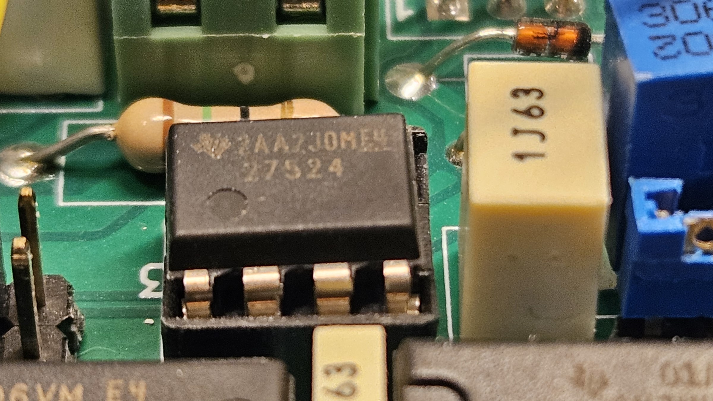
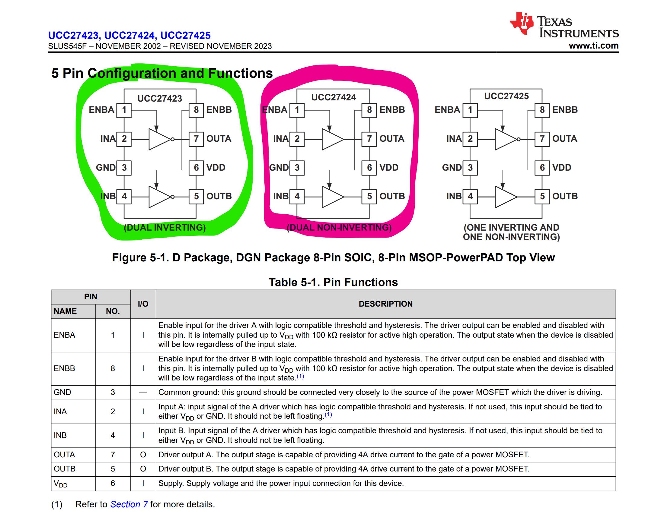

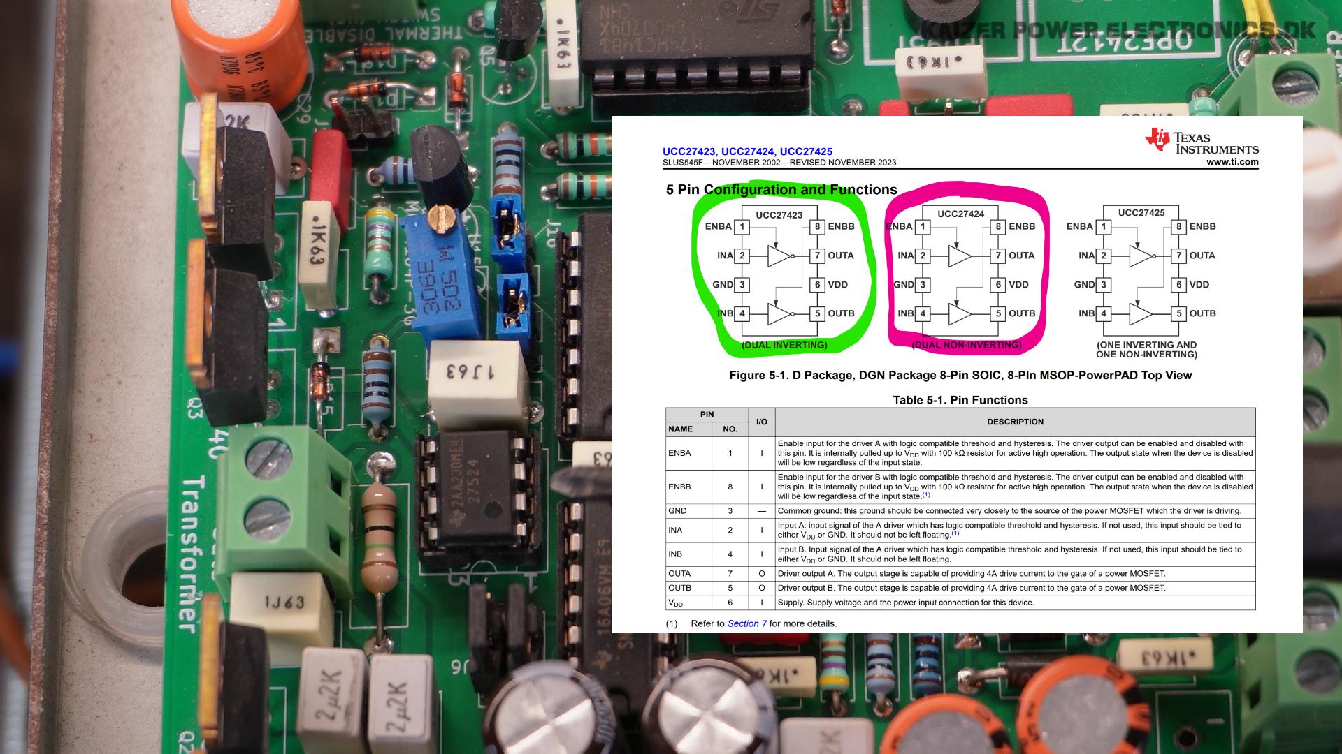
I also learned that this wrong gate driver IC could actually destroy the IGBTs, even without any supply on the DC bus. When bench testing the new full-bridges, gate drive waveform suddenly started acting weird and then flatlined. Short-circuit testing the full-bridge showed that it was damaged again. This damage was therefore already present in the previous episode, where I force the coil to run with a signal generator and the explosion is no longer a mystery 🙂
Destroyed Full-bridges, IGBT Test and New Bridges. The full-bridge that exploded in the previous episode, shows clearly that dies are completely melted on two IGBTs from lower and high side of the bridge. It is quite surprising that the packages did not even crack, yet are so melted into large blobs on the inside.
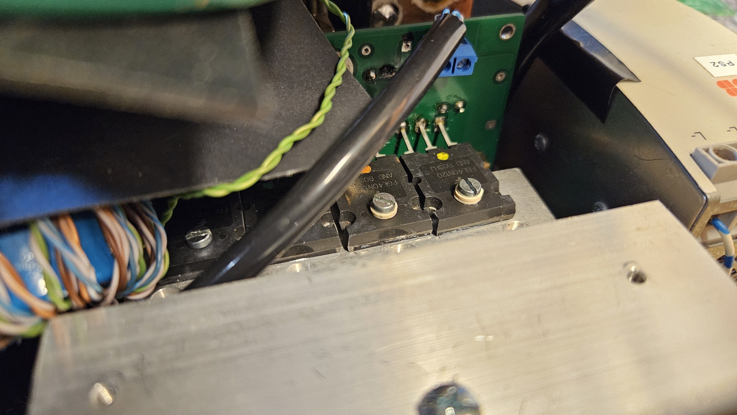
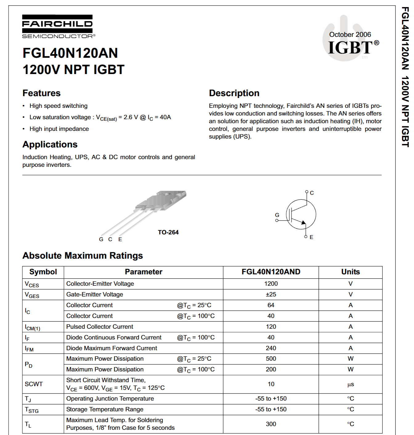
I only had enough 40N60 IGBTs to exchange both full-brigdes once. I wanted to compare the wrong IC vs. correct IC, but that actually destroyed the IGBTs in one of the bridges again. Having run out of 40N60, I had to substitute with some FGL40N120AN IGBTs, but these have lower current handling capability and higher gate capacitances, from the double voltage rating.
| Name | Voltage | Current (25C) | Peak Current | Vce(sat) | Switch losses Etotal (mJ) |
| 40N60 | 600 V | 80 A | 120 A | 2.5 V | 1.61 |
| FGL40N120AN | 1200 V | 40 A | 160 A | 2.6 V | 4.3 |
I changed the two small capacitors 0.1 uF and 0.47 uF, to a single large 10 uF snubber capacitor, to counter for the relatively high stray inductances in the full-bridges layout.
I added two pieces of copper wire, to bridge through the vias between the IGBTs, to get a better suited high current path for the resonant primary circuit.
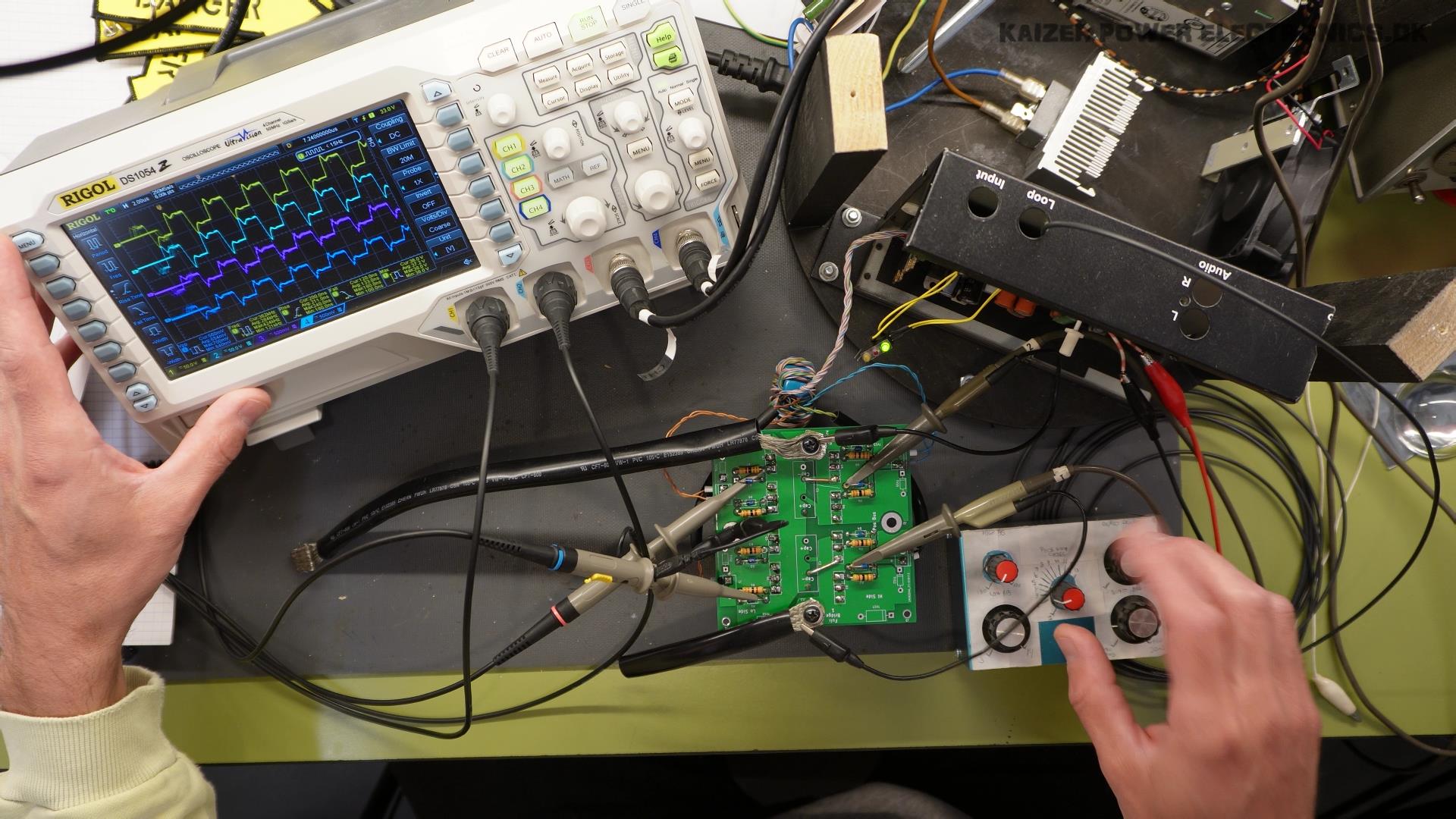
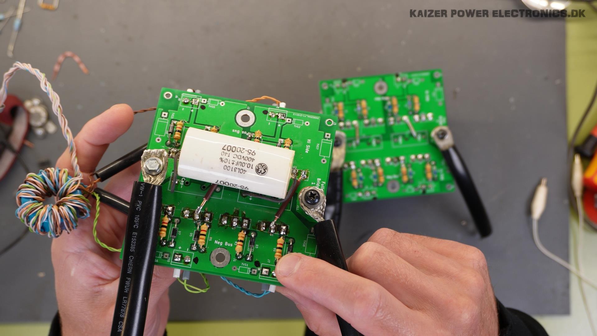
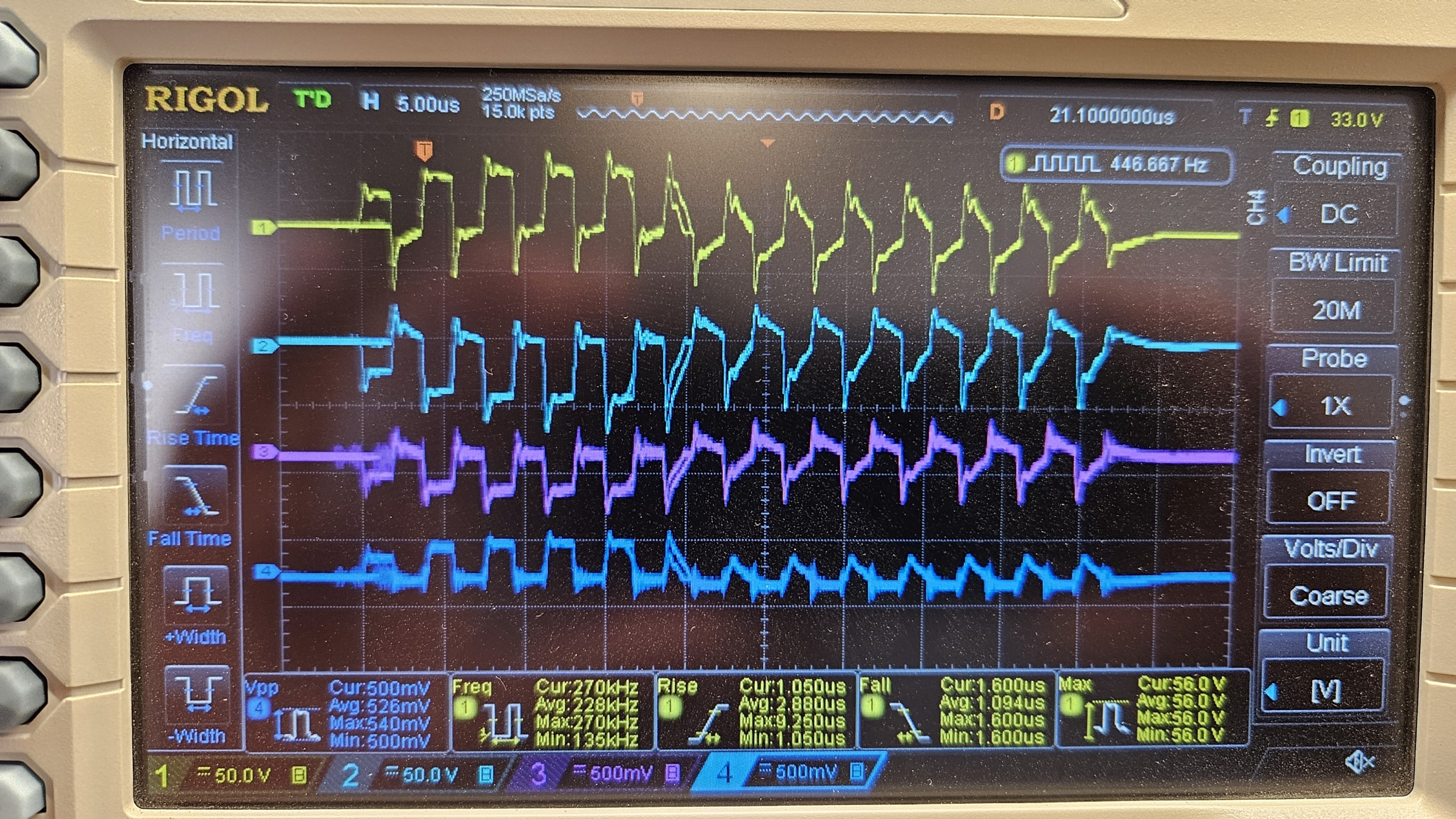
DRSSTC Primary Waveforms and Phase Lead Adjustment. Measurements with current monitors and differential probes is pretty straight forward. Place your current transformer on the lead from inverter output to primary circuit and place the differential probe for voltage measurement on the two inverter outputs.
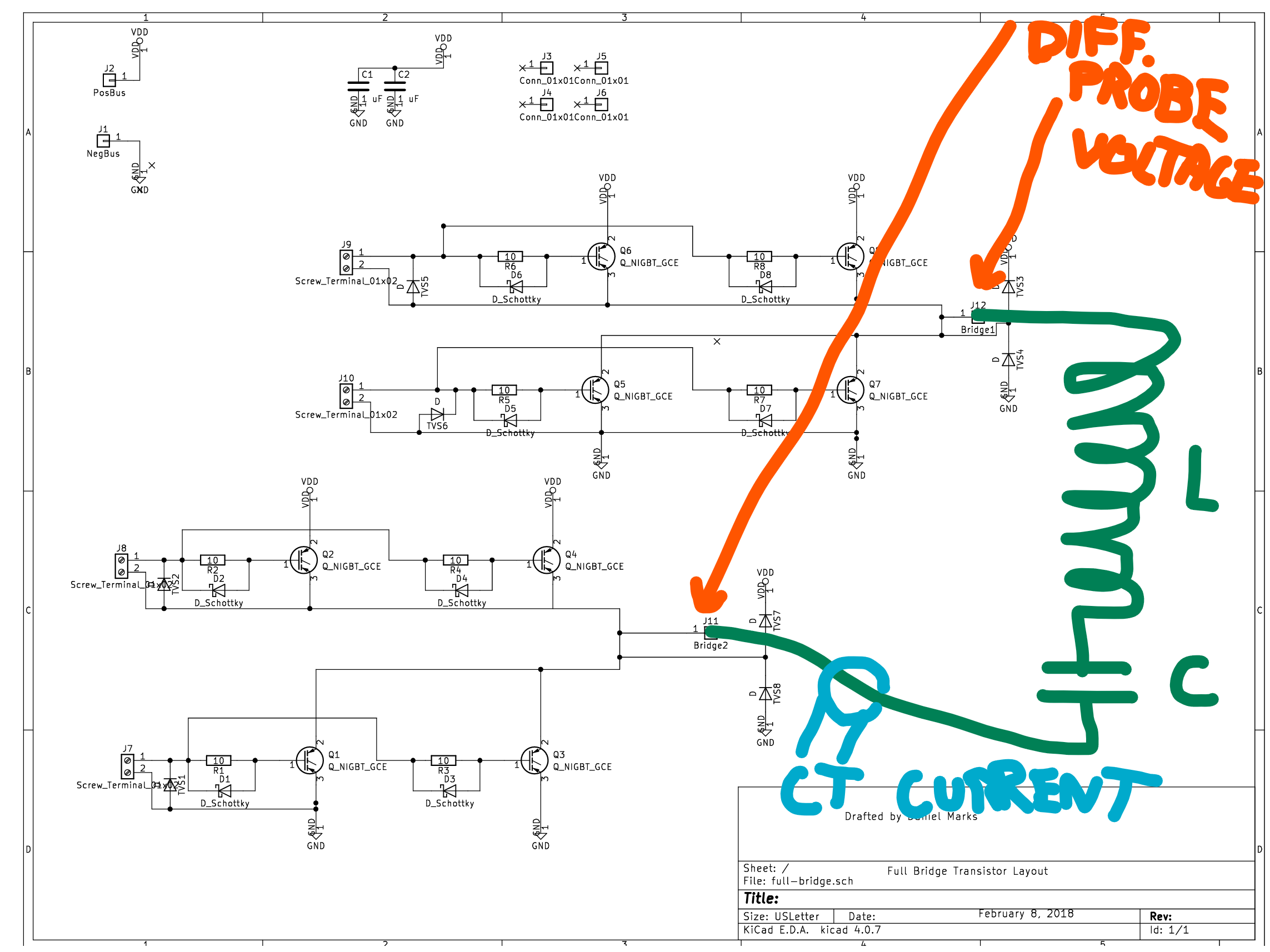
Alternative measurements, if you do not own expensive tools like current monitors and differential probes, is to use a normal 2-channel oscilloscope with 10x probes. You have to be very careful with placing the grounding clips correctly according to the schematics, else you short out your full-bridge lower leg.
For current measurement, place a probe across the shunt resistor R3 on the driver, excluding the inductor! This is important to not get phase
lead into your current signal that you are trying to “move” the voltage in regard to.
For the voltage measurement, place a probe across one of the lower leg IGBTs collector and emitter legs, the voltage here is only half of your DC bus. This does not represent voltage spikes on the high side of the full-bridge, but it should be sufficient to get a fair phase lead adjustment.

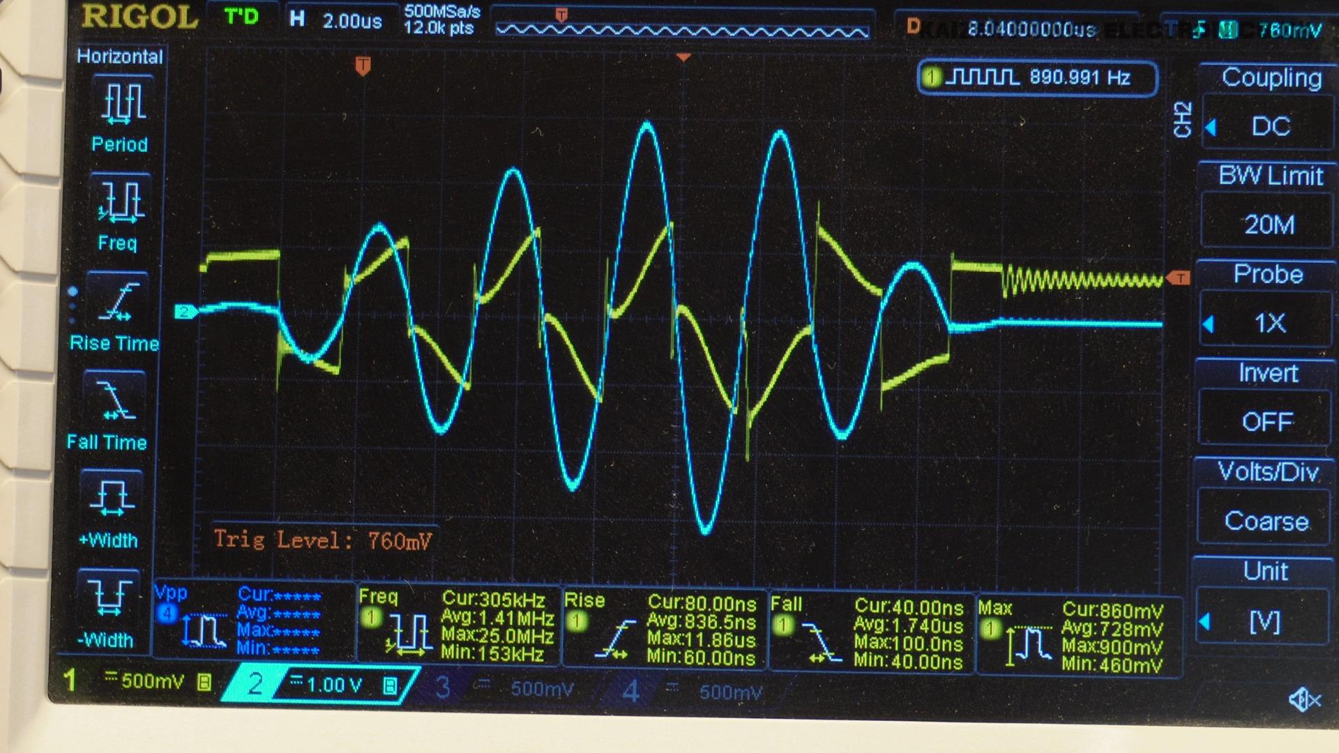
Blue trace is primary current with a scale of 100A/div and yellow trace is inverter output voltage with a scale of 250V/div. The primary current is in some screenshots set to 200A/div, in the screenshots where it is on level with the yellow trace.
The blue waveform shows the primary current ringing up and down. The yellow traces shows where the interrupter goes off again, the reverse voltage action is seen and the current is ringing down again from this point.
The sloped inverter output voltage waveform, is an indication of high stray inductances in the primary circuit layouts. The tracks or connections from DC bus capacitors to the primary coil connections, have to be as low inductance as possible. This PCB layout could use improvements in the track width and getting DC bus positive and negative tracks opposing each other, to cancel out the inductance.
The pulse skipping feature of the driver results in the OCD never really kicking in. The screenshot shows two pulse skipping events, the ringing current is halted by stopping the driver for one cycle, restarting from scratch and that results in what looks like 3 separate low duty-cycle pulses.
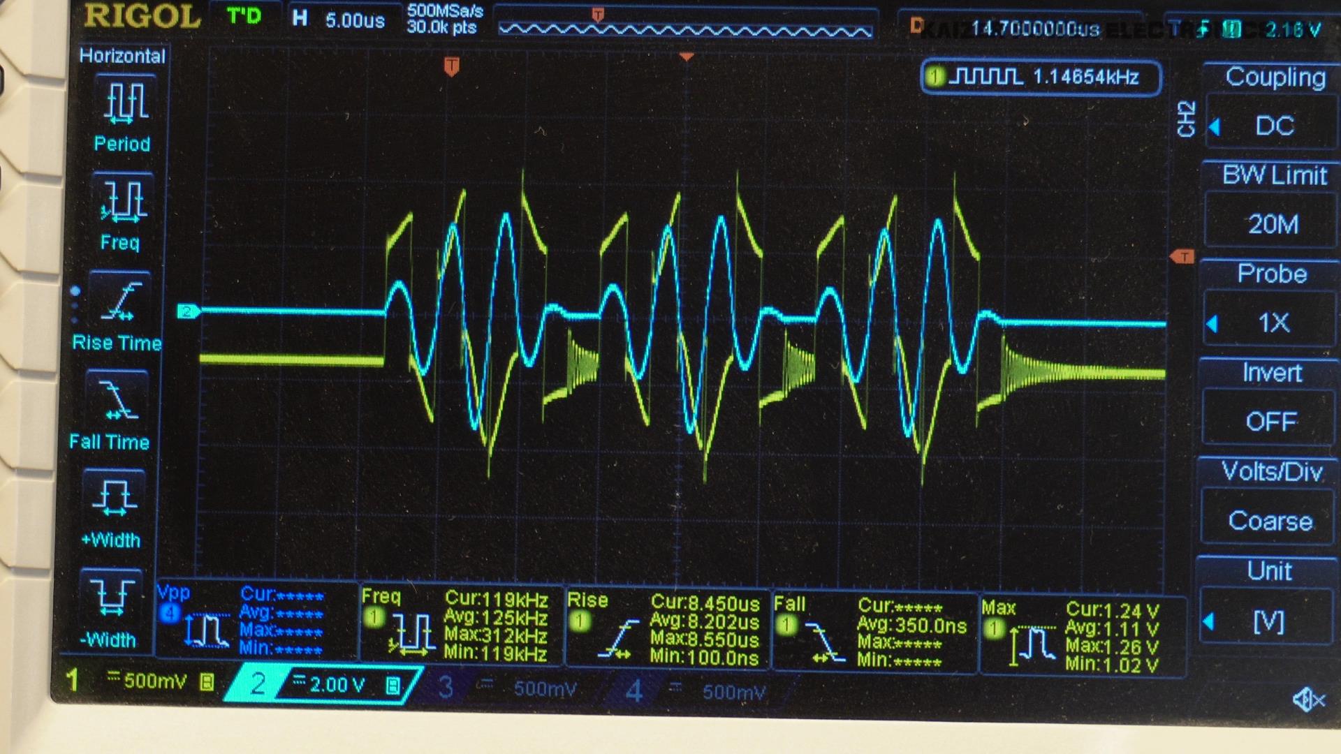
Phase lead adjustment is quite simple, you turn the adjustable inductor either left or right and watch the waveforms for a change. You want to find the spot where the spikes at the start of the voltage waveform is as low as possible.
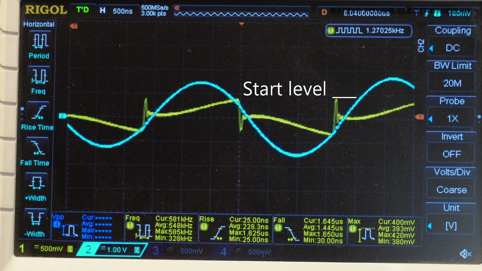
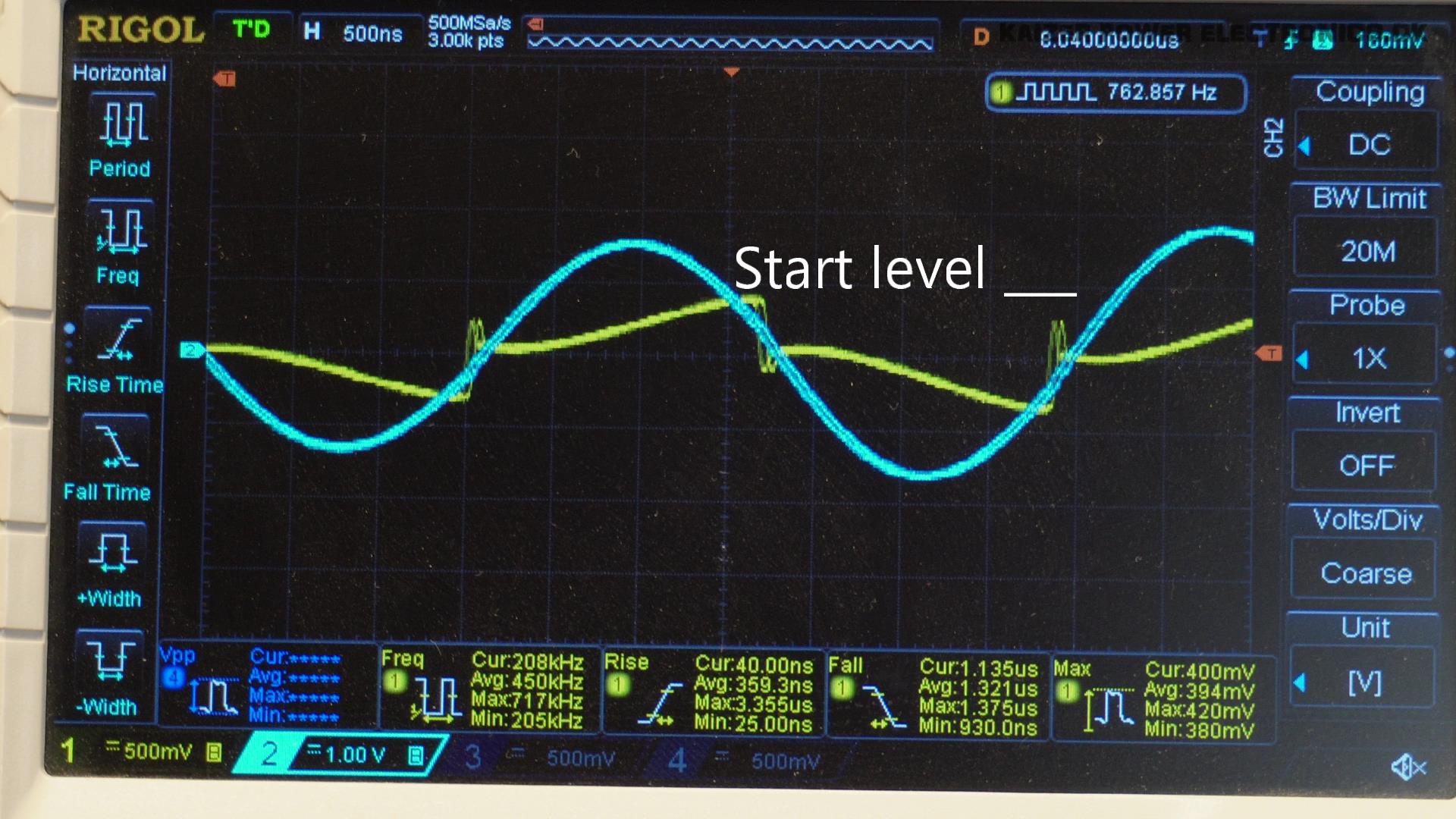
If adjusting the inductance is not making any change to the waveform, maybe the inductor size or type is not suitable. To check your variable inductor, you can use this calculator I made for this purpose: https://kaizerpowerelectronics.dk/calculators/ud2-x-phase-lead-calculator/
DRSSTC VII? Where is V and VI?
Those are designs and ideas, in a folder on my PC, so they get to wait for their turn 🙂