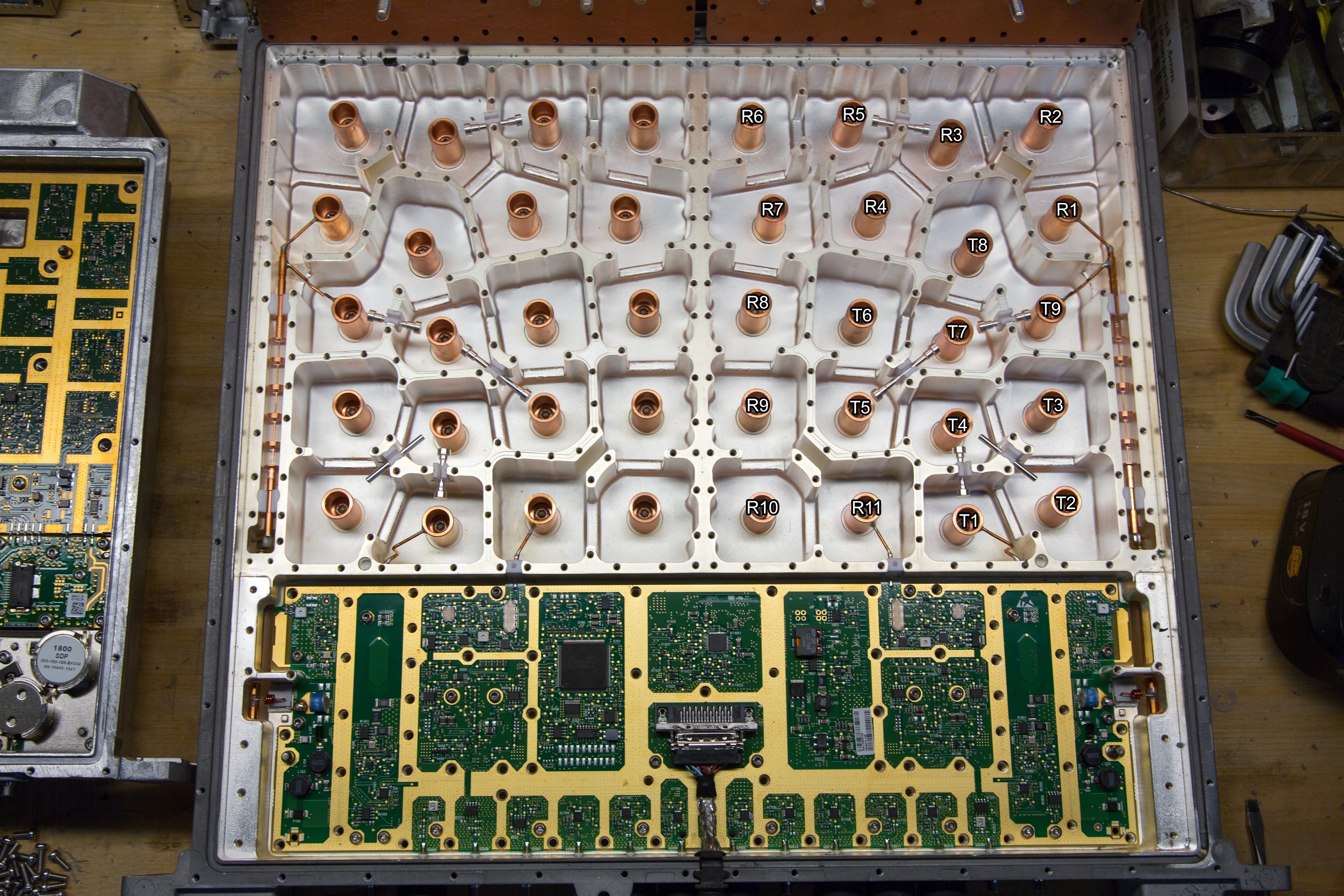
Circuit analysis of a Nokia Siemens Networks Flexi BTS base station. This have been in service as a 6 antenna GSM system for mobile telecommunications. GSM/EDGE, WCDMA/HSPA and LTE capable. 2×40 Watt output power.
If you missed part 1, see it here: https://kaizerpowerelectronics.dk/teardown/nokia-siemens-flexi-bts-base-station-teardown-power-amplifier-part-1-of-2/
Filter
Above picture shows the coaxial cavity band pass filter which in popular speech is called a duplexer or diplexer. For a explanation on how this works, watch the first part of the video shown here above.
System
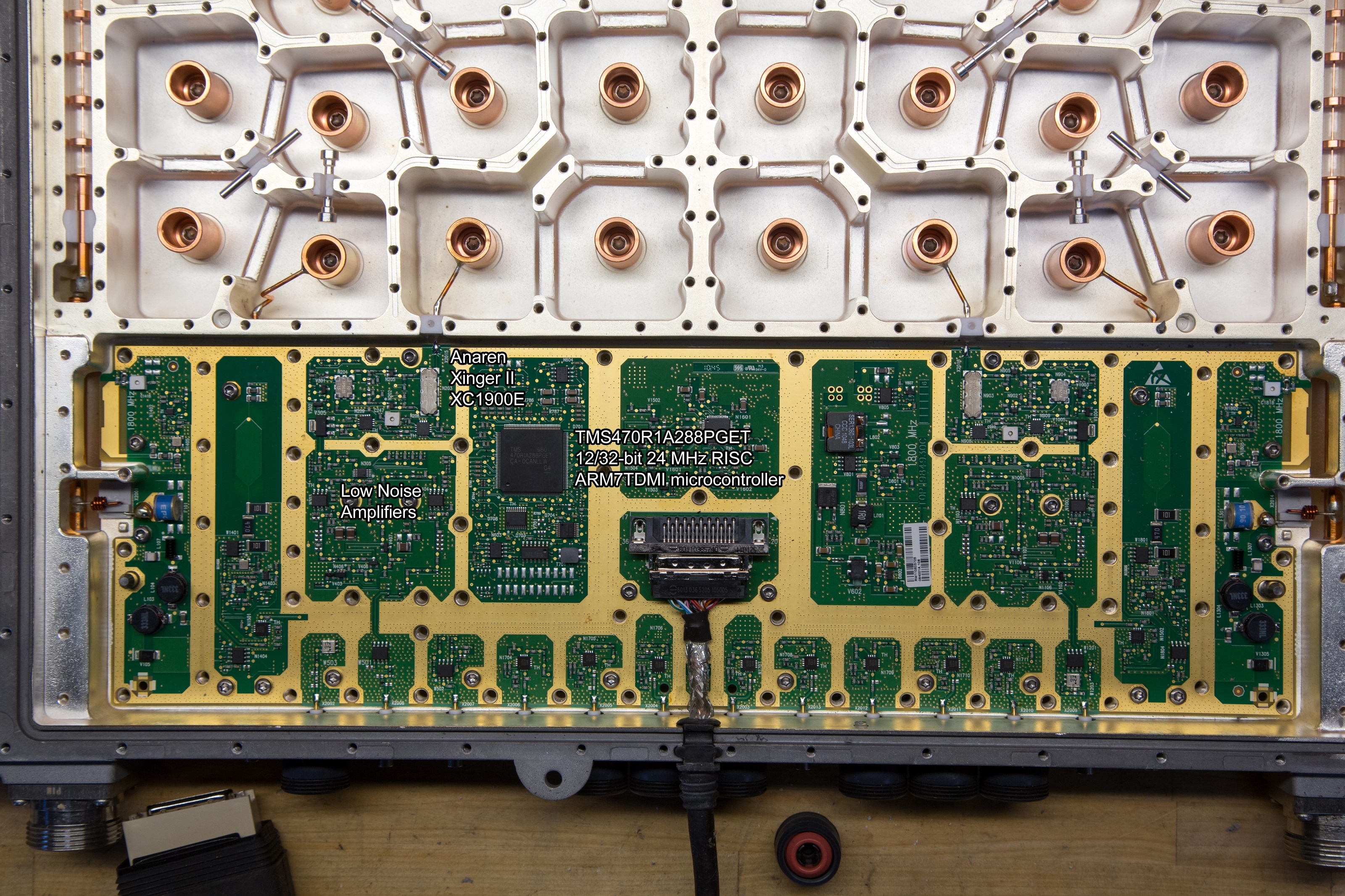
The duplexer control board and front end is managed by a ARM7 TDMI microcontroller with part number TMS470R1A288PGET. It is a 32-bit 24 MHz RISC processor.
Anaren Xinger II XC1900E hybrid couplers are used for phase split before feeding into the low noise amplifiers for signal transfer from duplexer module to power amplifier module.
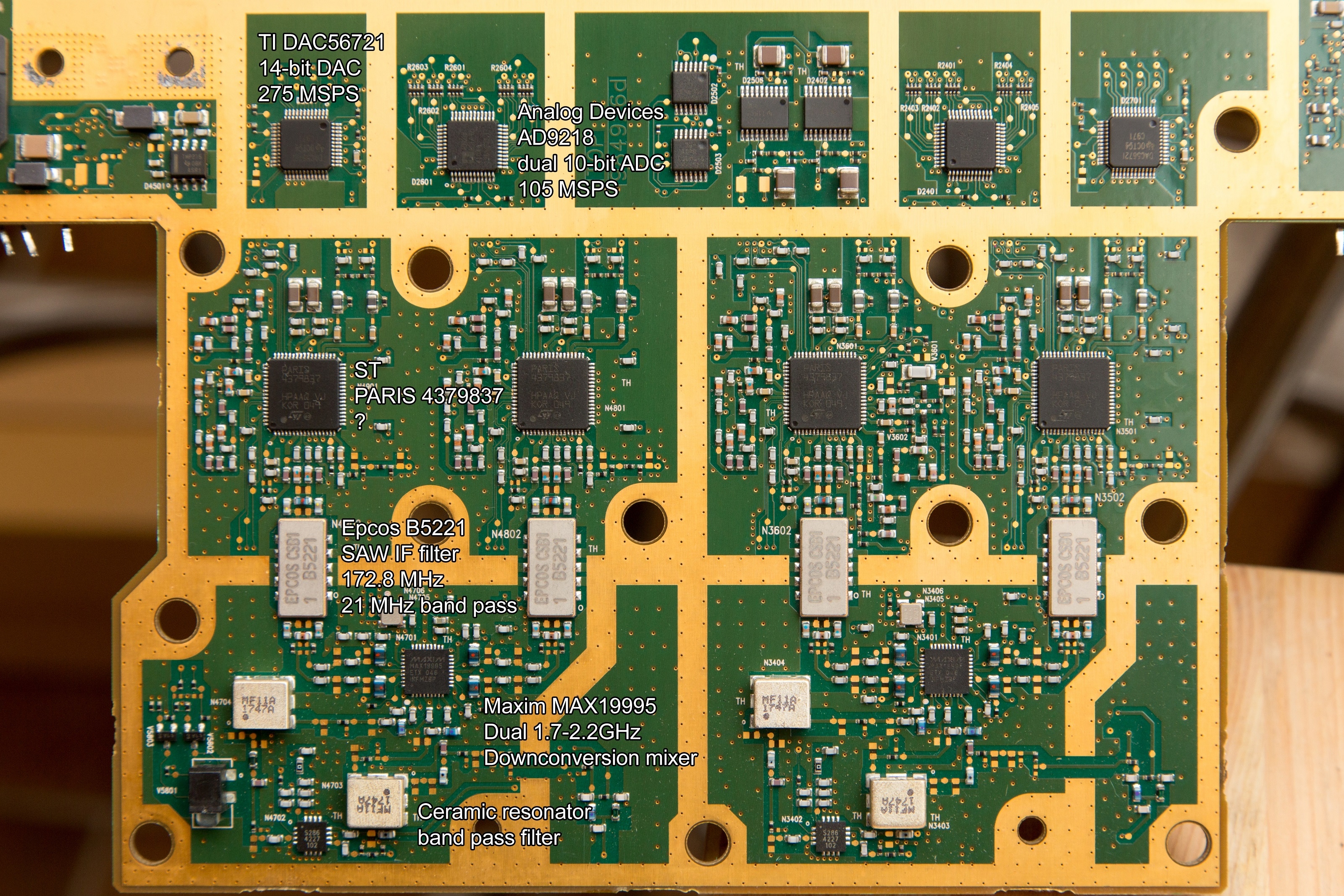
The last picture could possibly show the DAC used for the transmit chain. It is a TI DAC56721 which is a 14-bit DAC capable of 275 MSPS.
Power amplifier
The power amplifier consists of a series of low noise amplifiers, general purpose amplifiers and power amplifiers. The first few amplifier ICs are not able to be identified as their part numbers are not unique.
First identifiable IC is a Freescale M005N 0.8-2.2 GHz 18.5 dB general purpose amplifier that feeds the Freescale SW7IC18100N which is a power amplifier rated for 100 Watt dissipate at 1.8 GHz.
Two output circulators is used for double protection against reflected energy from the duplexer and antenna array.
System
The system board main processor is a unknown TI FPGA that has a generic Nokia Siemens part number which is not identifiable. It has a Marvell Alaska 88E1111 Gigabit network controller to handle the optical network interfaces.
A Texas Instruments TI DSP IC could be used for the first stage digital to analog conversion, purely guessed on from its location on the PCB. It is the TMS320TCI100 (C64x series) with is running at 720 MHz and is able of running 5760 MIPS.
The analog to digital signal path starts with a ceramic resonator band pass filter (explained here: https://youtu.be/h9-KhfQM3nI?t=729 ) which feed into a Maxim MAX19995 dual 1.7-2.2 GHz downconversion mixer (explained here: https://youtu.be/qO127zY3voE?t=865 ) which by the use of a local oscillator can bring down the carrier frequency of the signal to something lower that is easier to work with.
The two separate lines now go through the ultra low loss 21 MHz band pass filters from Epcos. The B5221 is a 172.8 MHz SAW IF filter (explained here: https://youtu.be/qO127zY3voE?t=963 ) before being fed into either a ADC or another mixer, the ST PARIS part is not identifiable.
The last stage is the Analog Devices AD9218 which is a dual 10-bit analog to digital conversion IC capable of 105 MSPS.


Pingback: Nokia Siemens Flexi BTS Power Amplifier Teardown