Nokia Siemens Networks Flexi Multiradio BTS is a GSM/EDGE, WCDMA/(I-)HSPA, and LTE base station. For use in mobile telecommunication antenna networks. A network that you use daily on your cellphone.
Part 1: System station, Part 2: Power Amplifier and Part 3: Antenna
The following 25 minute video shows the teardown step by step with explanations, high resolution pictures of content is further down this post.
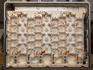
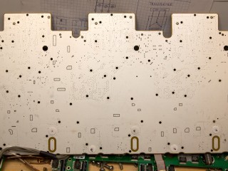
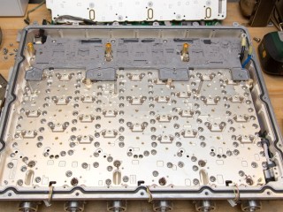
Diplexer
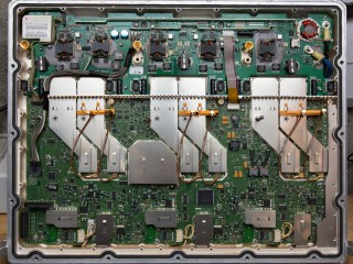
In the above pictures we see the tuning cavities of the band pass filter for the transmit and receive channels for the antenna connections. There is a total of three separate diplexers. Each diplexer / filter consists of a, from the left, receiving band pass filter and in the middle transmitting band pass filter. These two share the same antenna connection. At the right is another receiving band pass filter that has its own antenna connection.
The tuned cavities are machined in a whole piece of aluminium and silvered on the inside. The tuning pins in the top plate are all round brass pins. Additionally there is a stepper motor attached to copper metallized plastic parts, that can adjust the phase shift or filter response. This is not completely clear to me.
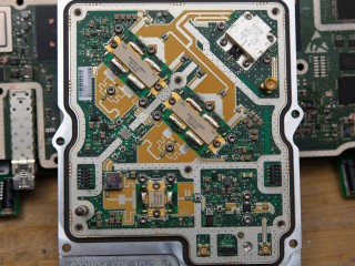
Power Amplifier
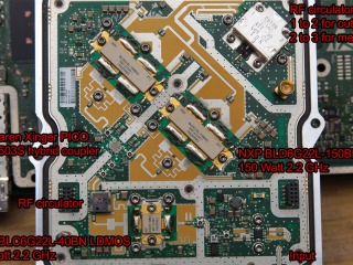
In the above pictures we see one of the three RF amplifier boards, there is a total of three of these boards. The board itself is a Aluminium Silicon Carbide heat sink on which all the components are directly mounted. The input connectors in the bottom of the pictures leads the signal through a small preamplifier (two screws on each side of a unmarked black package). Through an RF circulator to the NXP BLC6G22L-40BN integrated RF LDMOS which is a 2.2GHz 40 Watt amplifier. From here the signal is routed via another RF circulator to the Anaren Xinger PICO JP503S coupler. From here it distributes to the two output amplifiers. The last stage of amplification is handled by two BLC6G22L-150BN Power LDMOS transistors which are 2.2GHz 150 Watt transistors. In this setup, they are used for a combined 60 Watt output of the module. The output RF circulator is lead the signal to the output connector to the diplexer and any return signal is lead into a built in 50Ω attenuator.
System
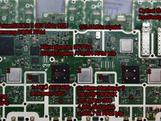
In the above pictures we see the digital/analogue signal processing board with the two optical inputs in the top right side of the picture. Digital data is processed by the Freescale / NXP MCP8347 PowerQUICC II 667 MHz CPU and its associated Xilinx Spartan II FPGA. Translation and splitting of the telecommunications protocol data and selection of different drive modes. If the amplifier is used for GSM, EDGE, HSPA, WCDMA or LTE, is done by the main computer setup described here. The digital to analogue for transmitting and analogue to digital for receiving is handled by the following setup.
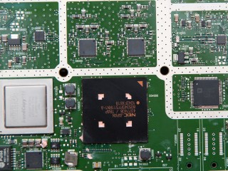
Receiving of data from the antennas are processed through the NEC 4377408 marked IC, that are impossible to locate any data on. They do however have great resemblance to the special Nokia Siemens Networks marked CPUs I have seen in other GSM/EDGE amplifiers. These handle the standard telecommunication protocol packaging and possible encryption of the digital datastream. The datastream comes from the two Analog Devices AD9238 12-bit 64MSPS analogue to digital converters that translates the analogue signal from the filter into a digital data stream.
Transmitting of data is handled by a Altera Hardcopy II, HC220F780NAK, ASIC. This translates the telecommunication protocol into a digital datastream that is fed to the Analog Devices AD9787 digital to analogue converter. This DAC has a speed of 800MSPS, from here the signal is led to the power amplifier board.
Filter
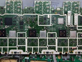
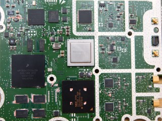
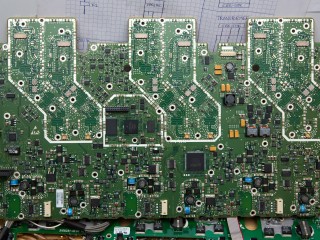
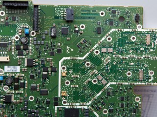
Between the system boards receiving part described above and the diplexer, is a signal processing and filtering board. The lower part of the board consists primarily of power supplies. A Lattice MachXO LCMX0640C that is a controller between CPLD and FPGA.
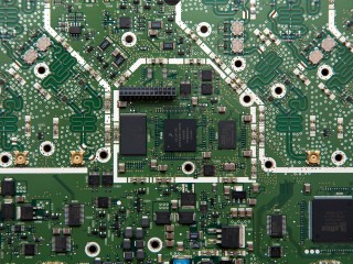
In the middle of the board, there is a shielded area that distinct itself from the 3 filtering areas. A NXP Coldfire MCF5208 166 MHz 32-bit CPU with DDR RAM and 10/100 ethernet controller is mounted here. Along side is its DDR RAM IC and ISSI IS42S16160D 64 MB 166 MHz SRAM.
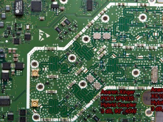
Each filter area consists of two channels that runs through carefully impedance matched paths. These paths are between the small amplifier ICs and Anaren Xinger PICO 1P503S 45W and Anaren Xinger II XC1900C-03S 160W couplers.
The filters seems to be designed for more than one frequency running along side another signal or more phase shifted signals of same frequency.
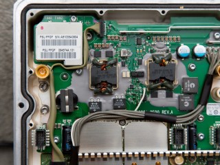
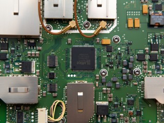
Power supply
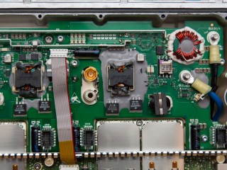
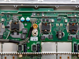
In the above pictures we can see the power supply board that is mounted above the filter board and this primarily supplies power to the 3 amplifiers.
It is a Emerson power supply board rated at 48 VDC / 28 Ampere.
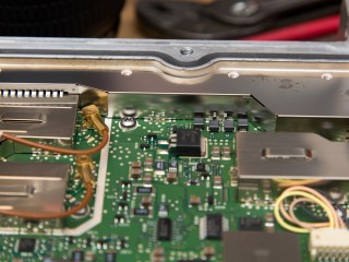
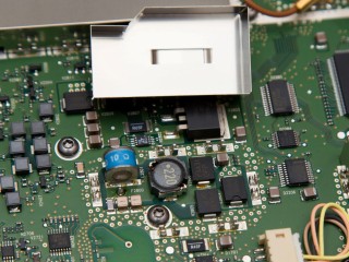
All shielding on the boards are neatly done with small spot welded boxes that are fixed in closely spaced clamping holders. These reminds me of small fuse holders. All the shields are easily removable, by a small raised slit in the top of it. Like a little handle, not a single shielding part was soldered to the board.
It is sensitive signals paths actually handling the RF signal, controllers and the magnetics of power supplies that are shielded individually.
Specifications
Frequency bands: 700, 800, 850, 900, 1800, 1900, 1700/2100, 2100, 2300 and 2600 MHz.
Maximum capacity: Up to 6+6+6 GSM or 4+4+4 WCDMA or 1+1+1 LTE at 20 MHz or flexible combination of the above technologies in concurrent mode.
Multi-radio configuration: 1 Flexi 3-sector RF module + 1 system module for GSM/EDGE + 1 system module for WCDMA/HSPA and LTE. Remote Radio Head (RRH) solution also supported.
RF power amplifier technology: Multicarrier power amplifier (multi-standard)
Height x width x depth: 133 x 447 x 560 mm per module, indoors and outdoors. Fits in any 19” rack.
Weight: 25 kg per module
Operating temperature range: -35 °C to +55 °C
Power supply: 40.5 – 57 VDC, 184 – 276 VAC with power module
Typical power consumption: 790W for combined GSM and WCDMA site
Output power: 240 W per RF module or 40 W + 40W per Remote Radio Head (RRH)
Ingress protection class: IP 65


Pingback: WCDMA Amplifier Teardown: Integrated Doherty Amplifier